Indice
~~BOZZA~~
L3-IP1
 Specialization card
Information
Release
| Document release | Description | Note | Date |
|---|---|---|---|
| 01 | New manual | Valid for hardware release 02 and above  | 20/03/2012 |
Descrizione
| Standard equipment | |
|---|---|
 | 8 PNP |
 | 8 500mA |
| Pin | Name | Description | Address | |
|---|---|---|---|---|
 | 1A | + 12 V | Voltage supplied 12 volt | - |
| 2 | I1 | Digital inputs (PNP) | X.INP01 | |
| 3 | I2 | X.INP02 | ||
| 4 | I3 | X.INP03 | ||
| 5 | I4 | X.INP04 | ||
| 6 | I5 | X.INP05 | ||
| 7 | I6 | X.INP06 | ||
| 8 | I7 | X.INP07 | ||
| 9 | I8 | X.INP08 | ||
| 10 | 0V | Voltage supplied 0V | - | |
| 11 | - | - | - | |
| 12 | - | - | - | |
| 13 | V+ | OUT 12 ÷ 28 Vdc | - | |
| 14 | O1 | Digital outputs (500 mA) | X.OUT02 | |
| 15 | O2 | X.OUT02 | ||
| 16 | O3 | X.OUT03 | ||
| 17 | O4 | X.OUT04 | ||
| 18 | O5 | X.OUT05 | ||
| 19 | O6 | X.OUT06 | ||
| 20 | O7 | X.OUT07 | ||
| 21 | O8 | X.OUT08 | ||
| 22 | V- | OUT 12 ÷ 28 Vdc | - |
Wiring example


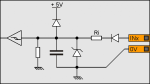
Digital inputs PNP
| Bias type | PNP |
|---|---|
| Min. acquisition time (hardware) | 3 ms |
| Opto-isolation | 1000 Vrms |
| Nominal voltage working | 12Vdc |
| Logic state 0 voltage | 0 ÷ 2V |
| Logic state 1 voltage | 10,5 ÷ 26,5 V |
| Internal Voltage drop | 5 V |
| Input resistance | 2700 W |
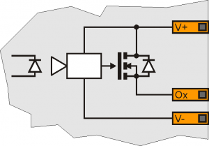
Digital outputs (500 mA)
| Commutate load | dc | (PNP) |
|---|---|---|
| Maximum operating voltage | 12 / 28 | Vdc |
| Opto-isolation | 1000 | Vpp |
| Max Internal Voltage drop | 0,5 | V |
| Max. resistance of MosFet | 0,5 | ohm |
| Max.current of protection | 700 | mA |
| Max.current function | 500 | mA |
| Off-state current | 10 | mA |
| Switching time from ON to OFF | 0,15 | ms |
| Switching time from OFF to ON | 0,10 | ms |
Programming information
Card declaration in BUS section of configuration unit:
| Slot number | Card software code | Firmware version |
|---|---|---|
| X | L3IP1 | 00 |
Example
BUS
1		983AF	01		;Slot 1
2		.			.			;Slot 2 (empty)
3		L3IP0	.			;Slot 3
4		.			.			;Slot 4 (empty)
Each hardware resource must be associated with the same address used in the electric description.
Example, if the card is installed in slot 3, the input X.INP01 must be associated to 3.INP01 address.
Example
(In configuration unit)
...
INPUT
ifLS_Max	F	3.INP01
...