Indice
Specialization card 1AD2F rel.03

Informations
| |
||||
| Document: | MIM1AD2F02 | |||
|---|---|---|---|---|
| Description: | Installation and maintenance manual | |||
| Editor: | Riccardo Furlato | |||
| Approver | Gabriele Bazzi | |||
| Link: | http://www.qem.eu/doku/doku.php/en/strumenti/qmoveplus/mim1AD2F02 | |||
| Language: | English | |||
| Document release | Hardware release | Description | Note | Date |
| 01 | 02 | New manual | 17/12/2014 | |
| 02 | 02 | Improved description of the analog input connector table and fixed the hardware release of the card | 18/06/2015 | |
| 03 | 02 | Fixed the SW3 setting description and examplex | 01/02/2016 | |
1. Description
The 1AD2F card of Qmove+ series.
1.1 Equipment
 | 8 digital inputs |
 | 2 multistandard analog inputs 16bit |
 | 8 digital outputs |
2. Connections
2.1 Digital inputs
2.1.1 8 digital inputs
| CN11 | Terminal | Simbol | Description | Address | |
|---|---|---|---|---|---|
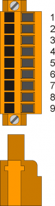 | 9 | 0V | Digital inputs common | ||
| 8 | I17 | Input I17 | 3.INP01 | ||
| 7 | I18 | Input I18 | 3.INP02 | ||
| 6 | I19 | Input I19 | 3.INP03 | ||
| 5 | I20 | Input I20 | 3.INP04 | ||
| 4 | I21 | Input I21 | 3.INP05 | ||
| 3 | I22 | Input I22 | 3.INP06 | ||
| 2 | I23 | Input I23 | 3.INP07 | ||
| 1 | I24 | Input I24 | 3.INP08 | ||
2.2 Analog inputs
2.2.1 2 multistandard analog inputs
Connector
| CN13 | Terminal | Simbol | Description | Address | ||
|---|---|---|---|---|---|---|
| Potentiometric / 0-10V / 0-20mA | Termocouple | PT100 | ||||
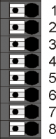 | 1 | GAI | Analog inputs common | - | - | |
| 2 | VREF | Reference volatege 1) | - | - | ||
| 3 | AI1_A | Analog input 1 | - | A 2) | 3.AI01 | |
| 4 | AI1_B | - | TC 1 - | B | ||
| 5 | AI1_C | - | TC 1 + | C | ||
| 6 | AI2_A | Analog input 2 | - | A 3) | 3.AI02 | |
| 7 | AI2_B | - | TC 2 - | B | ||
| 8 | AI2_C | - | TC 2 + | C | ||
Analog inputs setting
| Num. Dip | Analog input 1 | Analog input 2 | |||||||||
|---|---|---|---|---|---|---|---|---|---|---|---|
| PT100 | Termocouple | Pot. | 0-10V | 0-20mA | PT100 | Termocouple | Pot. | 0-10V | 0-20mA | ||
SW4 | 1 | ON | X | OFF | OFF | OFF | X | X | X | X | X |
| 2 | OFF | X | ON | ON | ON | X1) | X | X | X | X | |
| 3 | X | X | X | X | X | ON | X | OFF | OFF | OFF | |
| 4 | X2) | X | X | X | X | OFF | X | ON | ON | ON | |
| 5 | ON | ON | OFF | OFF | OFF | X | X | X | X | X | |
| 6 | OFF | OFF | ON | ON | ON | X | X | X | X | X | |
| 7 | OFF | ON | X | X | X | X | X | X | X | X | |
| 8 | X | X | X | X | X | OFF | ON | X | X | X | |
SW3 | 1 | X | X | X | X | X | X | X | OFF | OFF | ON |
| 2 | X | X | X | X | X | X | X | OFF | ON | OFF | |
| 3 | X | X | OFF | OFF | ON | X | X | X | X | X | |
| 4 | X | X | OFF | ON | OFF | X | X | X | X | X | |
X = setting not significant
Pot. = potentiometric type input
2.3 Digital outputs
2.3.1 8 protected digital outputs
| C12 | Terminal | Simbol | Description | Address |
|---|---|---|---|---|
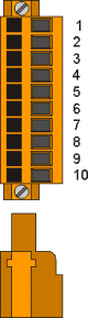 | 1 | V+ | Output power input (12÷28V dc) | |
| 2 | O17 | Digital output 17 | 3.OUT01 | |
| 3 | O18 | Digital output 18 | 3.OUT02 | |
| 4 | O19 | Digital output 19 | 3.OUT03 | |
| 5 | O20 | Digital output 20 | 3.OUT04 | |
| 6 | O21 | Digital output 21 | 3.OUT05 | |
| 7 | O22 | Digital output 22 | 3.OUT06 | |
| 8 | O23 | Digital output 23 | 3.OUT07 | |
| 9 | O24 | Digital output 24 | 3.OUT08 | |
| 10 | V- | Output power input (0V dc) |
3. Connection examples
3.1 Digital inputs

3.2 Potentiometric analog input 1 and voltmetric analog input 2

3.3 PT100 analog input 1 per and amperometric inputs 2

3.4 PT100 analog input 1 and termocouple analog input 2

3.5 Protected digital outputs

4. Electrical features
The following are the electrical hardware features.
The maximum and minimum frequency values and actual acquisition times, can still depend on any additional software filters, see the system variable “QMOVE:sys004”.
4.1 Digital inputs
| Type of polarisation | PNP |
| Min. acquisition time (hardware) | 3ms |
| Isolation | 1000Vrms |
| Rated operating voltage | 24Vdc |
| Voltage of logic state 0 | 0-2 V |
| Voltage of logic state 1 | 10.5 - 26.5 V |
| Internal voltage drop | 5V |
| Input resistance (Ri) | 2700Ω |
| Sink current | 2mA ÷ 8mA1) |
1)
CAUTION: If the device connected to the inputs needs a higher minimum current, inputs may not work properly.

4.2 Analog inputs
4.2.1 Conversion times
The electrical features depend on the type of input, configurable via DIP switch.
The conversion times from analog to digital depend on the configuration according to the table:
| Analog Input Configuration | Conversion time per channel |
|
|---|---|---|
| Input 1 | Input 2 | |
| DC1) | - | 4.6 ms |
| - | DC2) | 4.6 ms |
| DC3) | DC4) | 9.3 ms |
| DC5) | TC | 9.3 ms |
| DC6) | PT100 | 79.1 ms |
| TC | - | 9.3 ms |
| - | TC | 9.3 ms |
| TC | DC7) | 9.3 ms |
| TC | TC | 9.3 ms |
| TC | PT100 | 83.8 ms |
| PT100 | - | 74.5 ms |
| - | PT100 | 74.5 ms |
| PT100 | DC8) | 79.1 ms |
| PT100 | TC | 79.1 ms |
| PT100 | PT100 | 79.1 ms |
4.2.2 Amperometric analog inputs in 0-20mA configuration
| Connection type | Amperometric (0-20 mA) |
| Resolution | 12bit/16bit1) |
| Input resistance | 125Ω |
| Value of damage | 25 mA |
| Max. Linearity error | + 0,1% Vfs |
| Max. Offset error | + 0,1% Vfs |
| S.n. | 71 dB |
| Conversion time | It depends on the configuration of the analog input. See section Conversion times if present 2) |
| Isolation | 1000 Vrms |
1)
It depends on the Hardware versions
2)
The sampling time of the device must be equal or higher than the conversion time

4.2.3 Potentiometric analog input configuration
| Connection type | Potentiometric 1KΩ÷20KΩ |
| Resolution | 12bit/16bit1) |
| Reference voltage output | 2,5Vdc |
| Max output current from reference | 10mA |
| Input resistance | 10MΩ |
| Max. Linearity error | + 0,1% Vfs |
| Max. Offset error | + 0,1% Vfs |
| S.n. | 71 dB |
| Conversion time | It depends on the configuration of the analog input. See section Conversion times if present 2) |
| Isolation | 1000 Vrms |
1)
It depend on the Hardware versions
2)
The sampling time of the device must be equal or higher than the conversion time

4.2.4 Voltmetric analog input configuration
| Connection type | Voltmetrico 0÷10V |
| Resolution | 12bit/16bit1) |
| Input resistance (Rin) | 40KΩ |
| Value of damage | 20V |
| Max. Linearity error | + 0,1% Vfs |
| Max. Offset error | + 0,1% Vfs |
| S.n. | 71 dB |
| Conversion time | It depends on the configuration of the analog input. See section Conversion times if present 2) |
| Isolation | 1000 Vrms |
1)
It depends on the Hardware versions
2)
The sampling time of the device must be equal or higher than the conversion time

4.2.5 PT100 analog input configuration
| Sensor type collegabile | PT100 3 wire 1) |
| Measure type | Resistance 2) |
| Resolution | 15 bit (32767 corresponds to 250.00 O) |
| Input resistance (Rin) | 15 MO |
| Measuring current | 1 mA |
| Value of damage | 10V |
| Accuracy of resistance measurement | ± 0,04% |
| Conversion time | It depends on the configuration of the analog input. See section Conversion times if present 3) |
| Isolation | 1000 Vrms |
4.2.6 Termocouple analog input configuration
| Sensor type | Thermocouple type J,K,R,S,B,N,T,E 1) |
| Type of measure | Differential voltage |
| Resolution | 16 bit |
| Measuring range | ±156.25 mV |
| Measure for cold junction compensation | Integrated |
| Input resistance (Rin) | 15 MO |
| Value of damage | 30V |
| Measurement accuracy | ± 0,2% (excluding cold junction compensation) |
| Conversion time | It depends on the configuration of the analog input. See section Conversion times if present 2) |
| Isolation | 1000 Vrms |
4.2.7 Protected digital outputs
| Switchable load | Dc (PNP) |
| Max. operating voltage | 28V |
| Insulation | 1000VRMS |
| Max. internal voltage drop | 600mV |
| Max internal resistance @ON | 90mO |
| Max. protection current | 12A |
| Max. operating current | 500mA |
| Max. current @OFF | 5µA |
| Max switching time from ON to OFF | 270µs |
| Max switching time from OFF to ON | 250µs |
