Indice
Specialization card 1MG2F rel.01

Informations
| |
||||
| Document: | MIM1MG2F01 | |||
|---|---|---|---|---|
| Description: | Installation and maintenance manual | |||
| Editor: | Riccardo Furlato | |||
| Approver | Giuliano Tognon | |||
| Link: | http://www.qem.eu/doku/doku.php/en/strumenti/qmoveplus/mim1mg2f01 | |||
| Language: | English | |||
| Release documento | Hardware Release | Description | Note | Date |
| 00 | 01 | New document | 26/04/2016 | |
1. Description
The 1MG2F is a specialization card for the Qmove+ instrument.
1.1 standard equipment
 | 16 standard digital inputs (+4 inputs alternatively to 2 counters) |
 | 2 16bit multistandard analog inputs |
 | 2 bidirectional counters |
 | 16 digital outputs |
 | 2 analog outputs |
2. Techniques features
 Bisogna inserire un disegno con gli ingombri meccanici dell'espansione con la copertura
2.1 Mechanical dimensions
 | Measurements in mm |
|---|

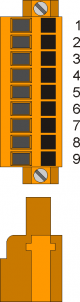
3. Connectors
3.1 Digital inputs
3.1.1 16 PNP digital inputs
| CN18 | Terminal | Simbol | Description | Address | |
|---|---|---|---|---|---|
 | 1 | 0V | Digital inputs common | ||
| 2 | I1 | Input I1 | 3.INP01 | ||
| 3 | I2 | Input I2 | 3.INP02 | ||
| 4 | I3 | Input I3 | 3.INP03 | ||
| 5 | I4 | Input I4 | 3.INP04 | ||
| 6 | I5 | Input I5 | 3.INP05 | ||
| 7 | I6 | Input I6 | 3.INP06 | ||
| 8 | I7 | Input I7 | 3.INP07 | ||
| 9 | I8 | Input I8 | 3.INP08 | ||
.
| CN19 | Terminal | Simbol | Description | Address | |
|---|---|---|---|---|---|
| | 1 | 0V | Digital inputs common | ||
| 2 | I9 | Input I9 | 3.INP09 | ||
| 3 | I10 | Input I10 | 3.INP10 | ||
| 4 | I11 | Input I11 | 3.INP11 | ||
| 5 | I12 | Input I12 | 3.INP12 | ||
| 6 | I13 | Input I13 | 3.INP13 | ||
| 7 | I14 | Input I14 | 3.INP14 | ||
| 8 | I15 | Input I15 | 3.INP15 | ||
| 9 | I16 | Input I16 | 3.INP16 | ||
3.1.2 2 bidirectional input counters 200KHz
 | The electrical features are given in section Electrical features. The connection examples are provided in section Connection examples |
|---|
.
| CN22 | >Terminal | Simbol | Description | Address | ||
|---|---|---|---|---|---|---|
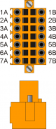 | 1A | +24V dc output 1) | ||||
| 2A | PHA1 | Phase A | Counter 1 PNP / Push-Pull2) | 3.INP17 | 3.CNT01 | |
| 3A | PHB1 | Phase B | 3.INP18 | |||
| 4A | Z1 | Z | 1.INT05 | |||
| 5A | 0V | Counter inputs common | ||||
| 6A | 0V | |||||
| 7A | 0V | |||||
| 1B | +24V dc output3) | |||||
| 2B | PHA1+ | + PHA | Counter 1 Line Driver | 3.INP17 | 3.CNT01 | |
| 3B | PHB1+ | + PHB | 3.INP18 | |||
| 4B | Z1+ | + Z | 1.INT05 | |||
| 5B | PHA1- | - PHA | ||||
| 6B | PHB1- | - PHB | ||||
| 7B | Z1- | - Z | ||||
5B terminal : to connect at 5A terminal
6B terminal: to connect at 6A terminal
7B terminal: to connect at 7A terminal
| CN21 | Terminal | Simbol | Description | Address | ||
|---|---|---|---|---|---|---|
| | 1A | +24V dc output1) | ||||
| 2A | PHA2 | Phase A | Conteggio 2 PNP / Push-Pull2) | 3.INP19 | 3.CNT02 | |
| 3A | PHB2 | Phase B | 3.INP20 | |||
| 4A | Z2 | Z | 1.INT06 | |||
| 5A | 0V | Counter inputs common | ||||
| 6A | 0V | |||||
| 7A | 0V | |||||
| 1B | +24V dc output3) | |||||
| 2B | PHA2+ | + PHA | Counter 2 Line Driver | 3.INP19 | 3.CNT02 | |
| 3B | PHB2+ | + PHB | 3.INP20 | |||
| 4B | Z2+ | + Z | 1.INT06 | |||
| 5B | PHA2- | - PHA | ||||
| 6B | PHB2- | - PHB | ||||
| 7B | Z2- | - Z | ||||
5B terminal : to connect at 5A terminal
6B terminal: to connect at 6A terminal
7B terminal: to connect at 7A terminal
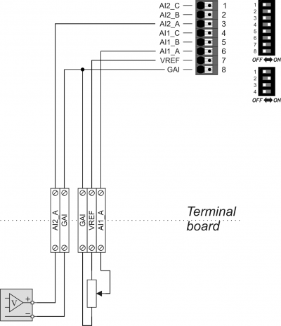
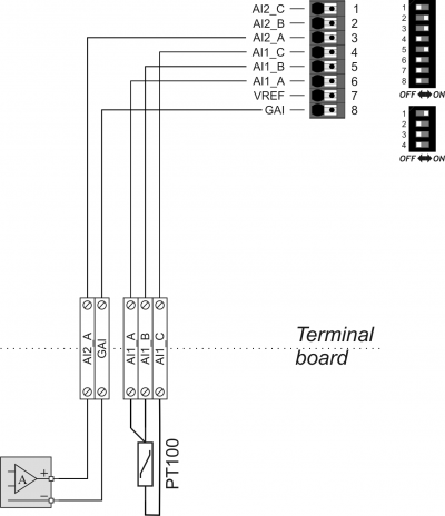
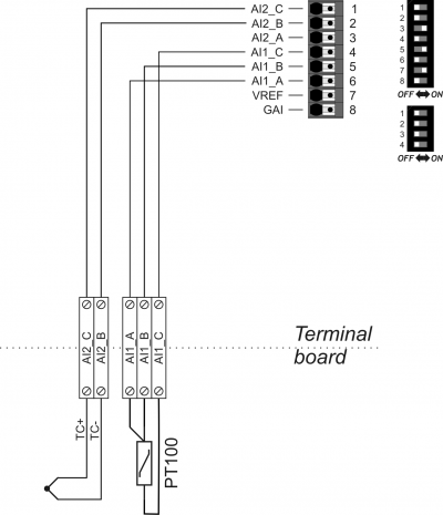
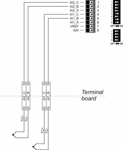
3.2 Analog inputs
3.2.1 2 multistandard analog inputs
Connector
Analog inputs setting
| Num. Dip | Analog input 1 | Analog input 2 | |||||||||
|---|---|---|---|---|---|---|---|---|---|---|---|
| PT100 | Thermocouple | Pot. | 0-10V | 0-20mA | PT100 | Thermocouple | Pot. | 0-10V | 0-20mA | ||
SW6 | 1 | ON | X | OFF | OFF | OFF | X | X | X | X | X |
| 2 | OFF | X | ON | ON | ON | X | X | X | X | X | |
| 3 | X | X | X | X | X | ON | X | OFF | OFF | OFF | |
| 4 | X | X | X | X | X | OFF | X | ON | ON | ON | |
| 5 | ON | ON | OFF | OFF | OFF | X | X | X | X | X | |
| 6 | OFF | OFF | ON | ON | ON | X | X | X | X | X | |
| 7 | OFF | ON | X | X | X | X | X | X | X | X | |
| 8 | X | X | X | X | X | OFF | ON | X | X | X | |
SW7 | 1 | X | X | X | X | X | X | X | OFF | OFF | ON |
| 2 | X | X | X | X | X | X | X | OFF | ON | OFF | |
| 3 | X | X | OFF | OFF | ON | X | X | X | X | X | |
| 4 | X | X | OFF | ON | OFF | X | X | X | X | X | |
X = irrelevant setting
Pot. = potentiometric type input
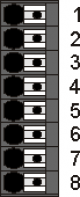
3.3 Digital outputs
3.3.1 16 protected digital outputs
| CN25 | Terminal | Simbol | Description | Address |
|---|---|---|---|---|
 | 1 | V+ | Outputs power O1÷O4 (12÷28V dc) | |
| 2 | O1 | Digital output 1 | 3.OUT01 | |
| 3 | O2 | Digital output 2 | 3.OUT02 | |
| 4 | O3 | Digital output 3 | 3.OUT03 | |
| 5 | O4 | Digital output 4 | 3.OUT04 | |
| 6 | V+ | Outputs power input O5÷O8(12÷28V dc) | ||
| 7 | O5 | Digital output 5 | 3.OUT05 | |
| 8 | O6 | Digital output 6 | 3.OUT06 | |
| 9 | O7 | Digital output 7 | 3.OUT07 | |
| 10 | O8 | Digital output 8 | 3.OUT08 | |
| 11 | V- | Outputs power input (0V dc) |
.
| CN20 | Terminal | Simbol | Description | Address |
|---|---|---|---|---|
| | 1 | V+ | Outputs power O9÷O12(12÷28V dc) | |
| 2 | O9 | Digital output 9 | 3.OUT09 | |
| 3 | O10 | Digital output 10 | 3.OUT10 | |
| 4 | O11 | Digital output 11 | 3.OUT11 | |
| 5 | O12 | Digital output 12 | 3.OUT12 | |
| 6 | V+ | Outputs power input O13÷O16(12÷28V dc) | ||
| 7 | O13 | Digital output 13 | 3.OUT13 | |
| 8 | O14 | Digital output 14 | 3.OUT14 | |
| 9 | O15 | Digital output 15 | 3.OUT15 | |
| 10 | O16 | Digital output 16 | 3.OUT16 | |
| 11 | V- | Outputs power input (0V dc) |
3.4 Analog outputs
3.4.1 2 +/-10V, 16bit analog outputs
| CN24 | Terminal | Simbol | Description | Address |
|---|---|---|---|---|
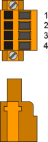 | 1 | GAO | Analog outputs common | |
| 2 | AO1 | Analog output 1 | 3.AN01 | |
| 3 | AO2 | Analog output 2 | 3.AN02 | |
| 4 | GAO | Analog outputs common |
4. Connection examples
4.1 Digital inputs

4.2 Line Driver counter inputs

4.3 PNP / Push Pull counter inputs

4.4 Analog inputs
4.4.1 Potentiometric input 1 and voltmetric input 2
4.4.2 PT100 input 1 and amperometric input 2
4.4.3 PT100 input 1 and termocouple input 2
4.4.4 Termocouple inputs 1 and 2
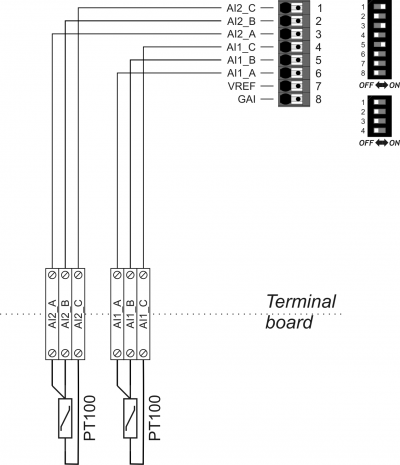
4.4.5 PT100 inputs 1 and 2
4.5 Protected digital outputs

4.6 Analog outputs

5. Electrical features
The following are the hardware electrical features .
Maximum and minimum frequency values and actual acquisition times, can depend on any additional software filters, for example to see the “QMOVE:sys004” system variable.
5.1 PNP digital inputs
| Type of polarisation | PNP |
| Min. acquisition time (hardware) | 3ms |
| Isolation | 1000Vrms |
| Rated operating voltage | 24Vdc |
| Voltage of logic state 0 | 0-2 V |
| Voltage of logic state 1 | 10.5 - 26.5 V |
| Internal voltage drop | 5V |
| Input resistance (Ri) | 2700Ω |
| Sink current | 2mA ÷ 8mA1) |

5.2 200KHz bidirectional counter inputs
The values given in the table refer to input signals A, B and Z.
The max. frequency given in the table refers to A and B phase signals with a DutyCycle = 50%
With count frequencies over 50KHz the use of Line-Driver type encoders is recommended.
| Type of polarisation | PNP/PP |
| Max frequency | 200KHz |
| Min. acquisition time | 5µs |
| Insulation | 1000Vrms |
| Rated operating voltage | 24Vdc |
| Voltage of logic status 0 | 0 - 2 V |
| Voltage of logic status 1 | 10.5 - 26.5 V |
| Internal voltage drop | 1.2V |
| Input resistance | 3100Ω |
Line-Driver
| Type of polarisation | Line-Driver |
| Max. frequency | 200KHz |
| Min. acquisition time | 5µs |
| Insulation | 1000Vrms |
| Rated operating voltage (PHx+ ? PHx-) | 5Vdc |
| Voltage of logic status 0 (PHx+ ? PHx-) | 0-1.5 V |
| Voltage of logic status 1 (PHx+ ? PHx-) | 2-5 V |
| Internal voltage drop | 1.2V |
| Input restistance | 150Ω |

5.3 Analog inputs
5.3.1 Conversion times
The electrical features depend on the type of input, configurable via DIP switch.
The conversion times from analog to digital depend on the configuration according to the table:
| Analog Input Configuration | Conversion time per channel |
|
|---|---|---|
| Input 1 | Input 2 | |
| DC1) | - | 4.6 ms |
| - | DC2) | 4.6 ms |
| DC3) | DC4) | 9.3 ms |
| DC5) | TC | 9.3 ms |
| DC6) | PT100 | 79.1 ms |
| TC | - | 9.3 ms |
| - | TC | 9.3 ms |
| TC | DC7) | 9.3 ms |
| TC | TC | 9.3 ms |
| TC | PT100 | 83.8 ms |
| PT100 | - | 74.5 ms |
| - | PT100 | 74.5 ms |
| PT100 | DC8) | 79.1 ms |
| PT100 | TC | 79.1 ms |
| PT100 | PT100 | 79.1 ms |
5.3.2 0-20mA analog input in amperometric configuration
| Connection type | Amperometric (0-20 mA) |
| Resolution | 12bit/16bit1) |
| Input resistance | 125Ω |
| Value of damage | 25 mA |
| Max. Linearity error | + 0,1% Vfs |
| Max. Offset error | + 0,1% Vfs |
| S.n. | 71 dB |
| Conversion time | It depends on the configuration of the analog input. See section Conversion times if present 2) |
| Isolation | 1000 Vrms |

5.3.3 Analog input in potentiometric configuration
| Connection type | Potentiometric 1KΩ÷20KΩ |
| Resolution | 12bit/16bit1) |
| Reference voltage output | 2,5Vdc |
| Max output current from reference | 10mA |
| Input resistance | 10MΩ |
| Max. Linearity error | + 0,1% Vfs |
| Max. Offset error | + 0,1% Vfs |
| S.n. | 71 dB |
| Conversion time | It depends on the configuration of the analog input. See section Conversion times if present 2) |
| Isolation | 1000 Vrms |

5.3.4 Analog input in voltmetric configuration
| Connection type | Voltmetrico 0÷10V |
| Resolution | 12bit/16bit1) |
| Input resistance (Rin) | 40KΩ |
| Value of damage | 20V |
| Max. Linearity error | + 0,1% Vfs |
| Max. Offset error | + 0,1% Vfs |
| S.n. | 71 dB |
| Conversion time | It depends on the configuration of the analog input. See section Conversion times if present 2) |
| Isolation | 1000 Vrms |

5.3.5 Analog input in PT100 configuration
| Sensor type collegabile | PT100 3 wire 1) |
| Measure type | Resistance 2) |
| Resolution | 15 bit (32767 corresponds to 250.00 O) |
| Input resistance (Rin) | 15 MO |
| Measuring current | 1 mA |
| Value of damage | 10V |
| Accuracy of resistance measurement | ± 0,04% |
| Conversion time | It depends on the configuration of the analog input. See section Conversion times if present 3) |
| Isolation | 1000 Vrms |
5.3.6 Analog input in termocouple configuration
| Sensor type | Thermocouple type J,K,R,S,B,N,T,E 1) |
| Type of measure | Differential voltage |
| Resolution | 16 bit |
| Measuring range | ±156.25 mV |
| Measure for cold junction compensation | Integrated |
| Input resistance (Rin) | 15 MO |
| Value of damage | 30V |
| Measurement accuracy | ± 0,2% (excluding cold junction compensation) |
| Conversion time | It depends on the configuration of the analog input. See section Conversion times if present 2) |
| Isolation | 1000 Vrms |
5.4 Protected digital outputs
| Switchable load | Dc (PNP) |
| Max. operating voltage | 28V |
| Insulation | 1000Vpp |
| Max. internal voltage drop | 600mV |
| Max internal resistance @ON | 90mΩ |
| Max. protection current | 12A |
| Max. operating current | 2A |
| Max. current @OFF | 5µA |
| Max switching time from ON to OFF | 270µs |
| Max switching time from OFF to ON | 250µs |

5.5 Analog outputs
| Type of connection | Common mode |
| Insulation | 1000Vrms |
| Voltage range (minimum no load) | -9.8V - +9.8V |
| Max. offset variation depending on temperature* | +/- 5mV |
| Resolution | 16bit |
| Max. current | 1mA |
| Output variation depending on load | 100 µV/mA |
| Output resistence | 249Ω |
