Indice
Specialization card 1MG6F rel.03

Informations
| |
||||
| Document: | MIM1MG6F03 | |||
|---|---|---|---|---|
| Description: | Installation and maintenance manual | |||
| Editor: | Riccardo Furlato | |||
| Approver | Gabriele Bazzi | |||
| Link: | http://www.qem.eu/doku/doku.php/en/strumenti/qmoveplus/mim1mg6f03 | |||
| Language: | English | |||
| Document release | Hardware release | Description | Note | Date |
| 00 | 03 | The step-direction voltage now are settable | 10/02/2016 | |
1. Description
The 1MG6F card for the Qmove+ series.
1.1 Equipment
 | 32 standard digital inputs (+12 alternative inputs to 6 counters) |
 | 4 analog inputs |
 | 4 rapid digital inputs |
 | 6 bidirectional counters |
 | 2 SSI absolute counters |
 | 32 digital outputs |
 | 8 analog outputs |
 | 5 step-direction outputs |
2. Connectors
2.1 Digital inputs
2.1.1 32 standard digital inputs + 4 rapid inputs
 | The electrical features are given in paragraph Electrical Features. The wiring examples are given in paragraph Connection examples |
|---|
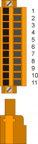
| CN11 | Terminal | Symbol | Description | Address | |
|---|---|---|---|---|---|
 | 1 | I01(PNP) | PNP type fast input I01 | External terminal configuration1) | FREQ12) |
| 2 | I01(NPN) | PNP type fast input I01 | |||
| 3 | 0V | Common for digital inputs | |||
| 4 | I1 | Input I1 | 3.INP01 | ||
| 5 | I2 | Input I2 | 3.INP02 | ||
| 6 | I3 | Input I3 | 3.INP03 | ||
| 7 | I4 | Input I4 | 3.INP04 | ||
| 8 | I5 | Input I5 | 3.INP05 | ||
| 9 | I6 | Input I6 | 3.INP06 | ||
| 10 | I7 | Input I7 | 3.INP07 | ||
| 11 | I8 | Input I8 | 3.INP08 | ||
| 12 | 0V | Common for digital inputs | |||
| CN12 | Terminal | Symbol | Description | Address | |
|---|---|---|---|---|---|
| | 1 | I02(PNP) | PNP type fast input I02 | External terminal configuration1) | FREQ22) |
| 2 | I02(NPN) | NPN type fast input I02 | |||
| 3 | 0V | Common for digital inputs | |||
| 4 | I9 | Input I9 | 3.INP09 | ||
| 5 | I10 | Input I10 | 3.INP10 | ||
| 6 | I11 | Input I11 | 3.INP11 | ||
| 7 | I12 | Input I12 | 3.INP12 | ||
| 8 | I13 | Input I13 | 3.INP13 | ||
| 9 | I14 | Input I14 | 3.INP14 | ||
| 10 | I15 | Input I15 | 3.INP15 | ||
| 11 | I16 | Input I16 | 3.INP16 | ||
| 12 | 0V | Common for digital inputs | |||
| CN13 | Terminal | Symbol | Description | Address | |
|---|---|---|---|---|---|
| | 1 | I03(PNP) | PNP type fast input I03 | External terminal configuration1) | 1.INT09 |
| 2 | I03(NPN) | NPN type fast input I03 | |||
| 3 | 0V | Common for digital inputs | |||
| 4 | I17 | Input I17 | 3.INP17 | ||
| 5 | I18 | Input I18 | 3.INP18 | ||
| 6 | I19 | Input I19 | 3.INP19 | ||
| 7 | I20 | Input I20 | 3.INP20 | ||
| 8 | I21 | Input I21 | 3.INP21 | ||
| 9 | I22 | Input I22 | 3.INP22 | ||
| 10 | I23 | Input I23 | 3.INP23 | ||
| 11 | I24 | Input I24 | 3.INP24 | ||
| 12 | 0V | Common for digital inputs | |||
1)
NPN type fast input configuration:
Terminal 1: connect to 12-24Vdc of the power unit
Terminal 2: input
PNP type fast input configuration:
Terminal 1: input
Terminal 2: connect to 0V (terminal 3)
Terminal 1: connect to 12-24Vdc of the power unit
Terminal 2: input
PNP type fast input configuration:
Terminal 1: input
Terminal 2: connect to 0V (terminal 3)
| CN14 | Terminal | Symbol | Description | Address | |
|---|---|---|---|---|---|
| | 1 | I04(PNP) | PNP type fast input I04 | External terminal configuration1) | 1.INT10 |
| 2 | I04(NPN) | NPN type fast input I04 | |||
| 3 | 0V | Common for digital inputs | |||
| 4 | I25 | Input I25 | 3.INP25 | ||
| 5 | I26 | Input I26 | 3.INP26 | ||
| 6 | I27 | Input I27 | 3.INP27 | ||
| 7 | I28 | Input I28 | 3.INP28 | ||
| 8 | I29 | Input I29 | 3.INP29 | ||
| 9 | I30 | Input I30 | 3.INP30 | ||
| 10 | I31 | Input I31 | 3.INP31 | ||
| 11 | I32 | Input I32 | 3.INP32 | ||
| 12 | 0V | Common for digital inputs | |||
1)
NPN type fast input configuration:
Terminal 1: connect to 12-24Vdc of the power unit
Terminal 2: input
PNP type fast input configuration:
Terminal 1: input
Terminal 2: connect to 0V (terminal 3)
Terminal 1: connect to 12-24Vdc of the power unit
Terminal 2: input
PNP type fast input configuration:
Terminal 1: input
Terminal 2: connect to 0V (terminal 3)
2.1.2 6 bidirectional counter inputs 200KHz
| The electrical features are given in paragraph Electrical features. The wiring examples are given in paragraph Connection examples |
|---|
| CN15 | Terminal | Symbol | Description | Address | ||
|---|---|---|---|---|---|---|
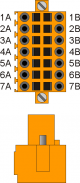 | 1A | Internal bridge 1A -1B | ||||
| 2A | PHA1 | Phase A count 1 | PNP Push-Pull1) | 3.INP33 | 3.CNT01 | |
| 3A | PHB1 | Phase B count 1 | 3.INP34 | |||
| 4A | Z1 | Z count 1 | 1.INT01 | |||
| 5A | 0V | Common for count inputs | ||||
| 6A | 0V | |||||
| 7A | 0V | |||||
| 1B | Internal bridge 1A -1B | |||||
| 2B | PHA1+ | + PHA count 1 | Line Driver | 3.INP33 | 3.CNT01 | |
| 3B | PHB1+ | + PHB count 1 | 3.INP34 | |||
| 4B | Z1+ | + Z count 1 | 1.INT01 | |||
| 5B | PHA1- | - PHA count 1 | ||||
| 6B | PHB1- | - PHB count 1 | ||||
| 7B | Z1- | - Z count 1 | ||||
1)
PNP/Push-Pull type count input configuration:
Terminal 5B: connect to terminal 5A
Terminal 6B: connect to terminal 6A
Terminal 7B: connect to terminal 7A
Terminal 5B: connect to terminal 5A
Terminal 6B: connect to terminal 6A
Terminal 7B: connect to terminal 7A
| CN16 | Terminal | Symbol | Description | Address | ||
|---|---|---|---|---|---|---|
| | 1A | Internal bridge 1A -1B | ||||
| 2A | PHA2 | Phase A count 2 | PNP Push-Pull1) | 3.INP35 | 3.CNT02 | |
| 3A | PHB2 | Phase B count 2 | 3.INP36 | |||
| 4A | Z2 | Z count 2 | 1.INT02 | |||
| 5A | 0V | Common for count inputs | ||||
| 6A | 0V | |||||
| 7A | 0V | |||||
| 1B | Internal bridge 1A -1B | |||||
| 2B | PHA2+ | + PHA count 2 | Line Driver | 3.INP35 | 3.CNT02 | |
| 3B | PHB2+ | + PHB count 2 | 3.INP36 | |||
| 4B | Z2+ | + Z count 2 | 1.INT02 | |||
| 5B | PHA2- | - PHA count 2 | ||||
| 6B | PHB2- | - PHB count 2 | ||||
| 7B | Z2- | - Z count 2 | ||||
1)
PNP/Push-Pull type count input configuration:
Terminal 5B: connect to terminal 5A
Terminal 6B: connect to terminal 6A
Terminal 7B: connect to terminal 7A
Terminal 5B: connect to terminal 5A
Terminal 6B: connect to terminal 6A
Terminal 7B: connect to terminal 7A
| CN17 | Terminal | Symbol | Description | Address | ||
|---|---|---|---|---|---|---|
| | 1A | Internal bridge 1A -1B | ||||
| 2A | PHA3 | Phase A count 3 | PNP Push-Pull1) | 3.INP37 | 3.CNT03 | |
| 3A | PHB3 | Phase B count 3 | 3.INP38 | |||
| 4A | Z3 | Z count 3 | 1.INT03 | |||
| 5A | 0V | Common for count inputs | ||||
| 6A | 0V | |||||
| 7A | 0V | |||||
| 1B | Internal bridge 1A -1B | |||||
| 2B | PHA3+ | + PHA count 3 | Line Driver | 3.INP37 | 3.CNT03 | |
| 3B | PHB3+ | + PHB count 3 | 3.INP38 | |||
| 4B | Z3+ | + Z count 3 | 1.INT03 | |||
| 5B | PHA3- | - PHA count 3 | ||||
| 6B | PHB3- | - PHB count 3 | ||||
| 7B | Z3- | - Z count 3 | ||||
1)
PNP/Push-Pull type count input configuration:
Terminal 5B: connect to terminal 5A
Terminal 6B: connect to terminal 6A
Terminal 7B: connect to terminal 7A
Terminal 5B: connect to terminal 5A
Terminal 6B: connect to terminal 6A
Terminal 7B: connect to terminal 7A
| CN18 | Terminal | Symbol | Description | Address | ||
|---|---|---|---|---|---|---|
| | 1A | Internal bridge 1A -1B | ||||
| 2A | PHA4 | Phase A count 4 | PNP Push-Pull1) | 3.INP39 | 3.CNT04 | |
| 3A | PHB4 | Phase B count 4 | 3.INP40 | |||
| 4A | Z4 | Z count 4 | 1.INT04 | |||
| 5A | 0V | Common for count inputs | ||||
| 6A | 0V | |||||
| 7A | 0V | |||||
| 1B | Internal bridge 1A -1B | |||||
| 2B | PHA4+ | + PHA count 4 | Line Driver | 3.INP39 | 3.CNT04 | |
| 3B | PHB4+ | + PHB count 4 | 3.INP40 | |||
| 4B | Z4+ | + Z count 4 | 1.INT04 | |||
| 5B | PHA4- | - PHA count 4 | ||||
| 6B | PHB4- | - PHB count 4 | ||||
| 7B | Z4- | - Z count 4 | ||||
1)
PNP/Push-Pull type count input configuration:
Terminal 5B: connect to terminal 5A
Terminal 6B: connect to terminal 6A
Terminal 7B: connect to terminal 7A
Terminal 5B: connect to terminal 5A
Terminal 6B: connect to terminal 6A
Terminal 7B: connect to terminal 7A
| CN19 | Terminal | Symbol | Description | Address | ||
|---|---|---|---|---|---|---|
| | 1A | Internal bridge 1A -1B | ||||
| 2A | PHA5 | Phase A count 5 | PNP Push-Pull1) | 3.INP41 | 3.CNT05 | |
| 3A | PHB5 | Phase B count 5 | 3.INP42 | |||
| 4A | Z5 | Z count 5 | 1.INT05 | |||
| 5A | 0V | Common for count inputs | ||||
| 6A | 0V | |||||
| 7A | 0V | |||||
| 1B | Internal bridge 1A -1B | |||||
| 2B | PHA5+ | + PHA count 5 | Line Driver | 3.INP41 | 3.CNT05 | |
| 3B | PHB5+ | + PHB count 5 | 3.INP42 | |||
| 4B | Z5+ | + Z count 5 | 1.INT05 | |||
| 5B | PHA5- | - PHA count 5 | ||||
| 6B | PHB5- | - PHB count 5 | ||||
| 7B | Z5- | - Z count 5 | ||||
1)
PNP/Push-Pull type count input configuration:
Terminal 5B: connect to terminal 5A
Terminal 6B: connect to terminal 6A
Terminal 7B: connect to terminal 7A
Terminal 5B: connect to terminal 5A
Terminal 6B: connect to terminal 6A
Terminal 7B: connect to terminal 7A
| CN20 | Terminal | Symbol | Description | Address | ||
|---|---|---|---|---|---|---|
| | 1A | Internal bridge 1A -1B | ||||
| 2A | PHA6 | Phase A count 6 | PNP Push-Pull1) | 3.INP43 | 3.CNT06 | |
| 3A | PHB6 | Phase B count 6 | 3.INP44 | |||
| 4A | Z6 | Z count 6 | 1.INT06 | |||
| 5A | 0V | Common for count inputs | ||||
| 6A | 0V | |||||
| 7A | 0V | |||||
| 1B | Internal bridge 1A -1B | |||||
| 2B | PHA6+ | + PHA count 6 | Line Driver | 3.INP43 | 3.CNT06 | |
| 3B | PHB6+ | + PHB count 6 | 3.INP44 | |||
| 4B | Z6+ | + Z count 6 | 1.INT06 | |||
| 5B | PHA6- | - PHA count 6 | ||||
| 6B | PHB6- | - PHB count 6 | ||||
| 7B | Z6- | - Z count 6 | ||||
1)
PNP/Push-Pull type count input configuration:
Terminal 5B: connect to terminal 5A
Terminal 6B: connect to terminal 6A
Terminal 7B: connect to terminal 7A
Terminal 5B: connect to terminal 5A
Terminal 6B: connect to terminal 6A
Terminal 7B: connect to terminal 7A
2.1.3 2 SSI absolute counters
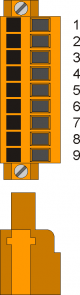
| CN22 | Terminal | Symbol | Description | Address |
|---|---|---|---|---|
| | 1A | Internal bridge 1A-2A-1B-2B | ||
| 2A | ||||
| 3A | DATA1+ | DATA in SSI1 | 1 | |
| 4A | DATA1- | |||
| 5A | CLOCK1+ | CLOCK out SSI1 | ||
| 6A | CLOCK1- | |||
| 7A | 0V | Common for count inputs | ||
| 1B | Internal bridge 1A-2A-1B-2B | |||
| 2B | ||||
| 3B | DATA2+ | DATA in SSI2 | 2 | |
| 4B | DATA2- | |||
| 5B | CLOCK2+ | CLOCK out SSI1 | ||
| 6B | CLOCK2- | |||
| 7B | 0V | Common for count inputs | ||
2.2 Analog inputs
2.2.1 4 potentiometric, voltmetric and amperometric analog inputs 12bit
| The electrical features are given in paragraph Electrical features. The wiring examples are given in paragraph Connection examples |
|---|
| CN28 | Terminal | Symbol | Description | Address |
|---|---|---|---|---|
 | 1 | GAI | Common for analog inputs | |
| 2 | IA1 | analog input 1 | 3.AI01 | |
| 3 | SEL1V | Analog input selector 1 voltmetric 0-10V1) | ||
| 4 | SEL1C | Analog input selector 1 amperometric 0-20mA2) | ||
| 5 | GAI | Common for analog inputs | ||
| 6 | IA2 | analog input 2 | 3.AI02 | |
| 7 | SEL2V | Analog input selector 2 voltmetric 0-10V3) | ||
| 8 | SEL2C | Analog input selector 2 amperometric 0-20mA4) | ||
| 9 | VREF | Reference voltage |
| CN29 | Terminal | Symbol | Description | Address |
|---|---|---|---|---|
| | 3 | GAI | Common for analog inputs | |
| 2 | IA3 | analog input 3 | 3.AI03 | |
| 3 | SEL3V | Analog input selector 3 voltmetric 0-10V1) | ||
| 4 | SEL3C | Analog input selector 3 amperometric 0-20mA2) | ||
| 5 | GAI | Common for analog inputs | ||
| 6 | IA4 | analog input 4 | 3.AI04 | |
| 7 | SEL4V | Analog input selector 4 voltmetric 0-10V3) | ||
| 8 | SEL4C | Analog input selector 4 amperometric 0-20mA4) | ||
| 9 | VREF | Reference voltage |
2.3 Digital outputs
2.3.1 32 protected digital outputs
| The electric features are listed on the paragraph Electric features. The example of the connections are listed on the Connection examples |
|---|
| CN7 | Terminal | Simbol | Description | Address |
|---|---|---|---|---|
 | 1 | V1+ | Input for outputs power supply O1÷O8 (12÷28V dc) | |
| 2 | O1 | Digital output 1 | 3.OUT01 | |
| 3 | O2 | Digital output 2 | 3.OUT02 | |
| 4 | V1- | Input for outputs power supply O1÷O8 (0V dc) | ||
| 5 | O3 | Digital output 3 | 3.OUT03 | |
| 6 | O4 | Digital output 4 | 3.OUT04 | |
| 7 | V1- | Input for outputs power supply O1÷O8 (0V dc) | ||
| 8 | O5 | Digital output 5 | 3.OUT05 | |
| 9 | O6 | Digital output 6 | 3.OUT06 | |
| 10 | O7 | Digital output 7 | 3.OUT07 | |
| 11 | O8 | Digital output 8 | 3.OUT08 |
| CN8 | Terminal | Simbol | Description | Address |
|---|---|---|---|---|
| | 1 | V2+ | Input for outputs power supply O9÷O16 (12÷28V dc) | |
| 2 | O9 | Digital output 9 | 3.OUT09 | |
| 3 | O10 | Digital output 10 | 3.OUT10 | |
| 4 | V2- | Input for outputs power supply (0V dc) | ||
| 5 | O11 | Digital output 11 | 3.OUT11 | |
| 6 | O12 | Digital output 12 | 3.OUT12 | |
| 7 | V2- | Input for outputs power supply O9÷O16 (0V dc) | ||
| 8 | O13 | Digital output 13 | 3.OUT13 | |
| 9 | O14 | Digital output 14 | 3.OUT14 | |
| 10 | O15 | Digital output 15 | 3.OUT15 | |
| 11 | O16 | Digital output 16 | 3.OUT16 |
| CN9 | Terminal | Simbol | Description | Address |
|---|---|---|---|---|
| | 1 | V3+ | Input for outputs power supply O17÷O24 (12÷28V dc) | |
| 2 | O17 | Digital output 17 | 3.OUT17 | |
| 3 | O18 | Digital output 18 | 3.OUT18 | |
| 4 | V3- | Input for outputs power supply O17÷O24 (0V dc) | ||
| 5 | O19 | Digital output 19 | 3.OUT19 | |
| 6 | O20 | Digital output 20 | 3.OUT20 | |
| 7 | V3- | Input for outputs power supply O17÷O24 (0V dc) | ||
| 8 | O21 | Digital output 21 | 3.OUT21 | |
| 9 | O22 | Digital output 22 | 3.OUT22 | |
| 10 | O23 | Digital output 23 | 3.OUT23 | |
| 11 | O24 | Digital output 24 | 3.OUT24 |
| CN10 | Terminal | Simbol | Description | Address |
|---|---|---|---|---|
| | 1 | V4+ | Input for outputs power supply O25÷O32 (12÷28V dc) | |
| 2 | O25 | Digital output 25 | 3.OUT25 | |
| 3 | O26 | Digital output 26 | 3.OUT26 | |
| 4 | V4- | Input for outputs power supply O25÷O32 (0V dc) | ||
| 5 | O27 | Digital output 27 | 3.OUT27 | |
| 6 | O28 | Digital output 28 | 3.OUT28 | |
| 7 | V4- | Input for outputs power supply O25÷O32 (0V dc) | ||
| 8 | O29 | Digital output 29 | 3.OUT29 | |
| 9 | O30 | Digital output 30 | 3.OUT30 | |
| 10 | O31 | Digital output 31 | 3.OUT31 | |
| 11 | O32 | Digital output 32 | 3.OUT32 |
2.3.2 5 STEP-DIRECTION outputs
| The electrical features are given in section Electrical features. The example of the connection are given in section Connection examples |
|---|
| CN23 | Terminal | Simbol | Description | Address | |
|---|---|---|---|---|---|
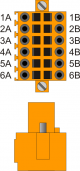 | 1A | VD1 | Internal bridge 1A -1B | ||
| 2A | DIR1+ | DIRECTION 1 output | Push-Pull Line Driver | 3.PULSE01 | |
| 3A | STEP1+ | STEP 1 output | |||
| 4A | DIR2+ | DIRECTION 2 output | 3.PULSE02 | ||
| 5A | STEP2+ | STEP 2 output | |||
| 6A | 0V | Stepper outputs common | |||
| 1B | VD1 | Internal bridge 1A -1B | |||
| 2B | DIR1- | DIRECTION 1 complementary output | Complementary outputs for use on driver with Line-Driver inputs | ||
| 3B | STEP1- | STEP 1 complementary output | |||
| 4B | DIR2- | DIRECTION 2 complementary output | |||
| 5B | STEP2- | STEP 2 complementary output | |||
| 6B | 0V | Stepper outputs common | |||
| CN24 | Terminal | Simbol | Description | Address | |
|---|---|---|---|---|---|
| | 1A | VD2 | Internal bridge 1A -1B | ||
| 2A | DIR3+ | DIRECTION 3 output | Push-Pull Line Driver | 3.PULSE03 | |
| 3A | STEP3+ | STEP 3 output | |||
| 4A | DIR4+ | DIRECTION 4 output | 3.PULSE04 | ||
| 5A | STEP4+ | STEP 4 output | |||
| 6A | 0V | Stepper outputs common | |||
| 1B | VD2 | Internal bridge 1A -1B | |||
| 2B | DIR3- | DIRECTION 3 complementary output | Complementary outputs for use on driver with Line-Driver inputs | ||
| 3B | STEP3- | STEP 3 complementary output | |||
| 4B | DIR4- | DIRECTION 4 complementary output | |||
| 5B | STEP4- | STEP 4 complementary output | |||
| 6B | 0V | Stepper outputs common | |||
| CN25 | Terminal | Simbol | Description | Address | |
|---|---|---|---|---|---|
| | 1A | VD3 | Internal bridge 1A -1B | ||
| 2A | DIR5+ | DIRECTION 5 output | Push-Pull Line Driver | 3.PULSE05 | |
| 3A | STEP5+ | STEP 5 output | |||
| 4A | - | n.c. | |||
| 5A | - | n.c. | |||
| 6A | 0V | Stepper outputs common | |||
| 1B | VD3 | Internal bridge 1A -1B | |||
| 2B | DIR5- | DIRECTION 5 complementary output | Complementary outputs for use on driver with Line-Driver inputs | ||
| 3B | STEP5- | STEP 5 complementary output | |||
| 4B | - | n.c. | |||
| 5B | - | n.c. | |||
| 6B | 0V | Stepper outputs common | |||
With JP1 to JP9 jumper, you can set the nominal voltage of the STEP and DIR outputs.
 | For each connector should be inserted only one bridge at a time If you select one of the two voltages 5V(JP3,JP6,JP9) or 12V(JP1,JP4,JP7) the 1A and 1B terminals must be disconnected |
|---|
.
| Name jumper | Setting | Nominal voltage | |
|---|---|---|---|
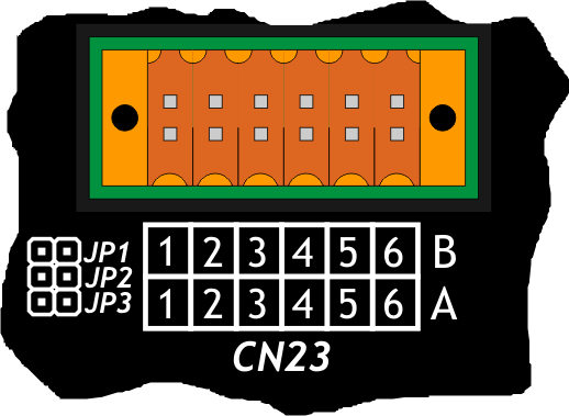 | JP1 | INSERTED | 12V (voltage supplied by the device) |
| JP2 | INSERTED | VD1 (Voltage to be supplied to terminals 1A or 1B) | |
| JP3 | INSERTED | 5V (Voltage supplied by the device) | |
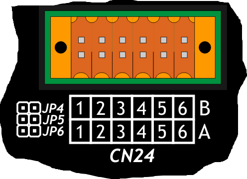 | JP4 | INSERTED | 12V (voltage supplied by the device) |
| JP5 | INSERTED | VD2 (Voltage to be supplied to terminals 1A or 1B) | |
| JP6 | INSERTED | 5V (Voltage supplied by the device) | |
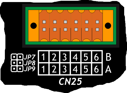 | JP7 | INSERTED | 12V (voltage supplied by the device) |
| JP8 | INSERTED | VD3 (Voltage to be supplied to terminals 1A or 1B) | |
| JP9 | INSERTED | 5V (Voltage supplied by the device) |
 | JP1,JP4,JP7 |
| JP2,JP5,JP8 | |
| JP3,JP6,JP9 |
2.4 Analog outputs
2.4.1 8 analog outputs +/-10V, 16bit
| The electrical features are given in paragraph Electrical features. The wiring examples are given in paragraph Connection examples |
|---|
| CN26 | Terminal | Symbol | Description | Address |
|---|---|---|---|---|
 | 1 | GAO | Common for analog outputs | |
| 2 | AO1 | Analog output 1 | 3.AN01 | |
| 3 | AO2 | Analog output 2 | 3.AN02 | |
| 4 | GAO | Common for analog outputs | ||
| 5 | AO3 | Analog output 3 | 3.AN03 | |
| 6 | AO4 | Analog output 4 | 3.AN04 |
| CN27 | Terminal | Symbol | Description | Address |
|---|---|---|---|---|
| | 1 | GAO | Common for analog outputs | |
| 2 | AO5 | Analog output 5 | 3.AN05 | |
| 3 | AO6 | Analog output 6 | 3.AN06 | |
| 4 | GAO | Common for analog outputs | ||
| 5 | AO7 | Analog output 7 | 3.AN07 | |
| 6 | AO8 | Analog output 8 | 3.AN08 |
3. Connection examples
3.1 Digital inputs

3.2 Line Driver counter inputs

3.3 PNP / Push Pull counter inputs

3.4 SSI absolute counters

3.5 Voltmetric and amprometric analog inputs

3.6 Voltmetric and potentiometric analog inputs

3.7 Protected digital outputs

3.8 STEP - DIRECTION outputs 12V

3.9 STEP - DIRECTION outputs 24V

3.10 Analog outputs

4. Electrical features
The following are the electrical hardware features.
The maximum and minimum frequency values and actual acquisition times, can still depend on any additional software filters, see the system variable “QMOVE:sys004”.
4.0.1 Standard digital inputs
| Type of polarisation | PNP |
| Min. acquisition time (hardware) | 3ms |
| Isolation | 1000Vrms |
| Rated operating voltage | 24Vdc |
| Voltage of logic state 0 | 0-2 V |
| Voltage of logic state 1 | 10.5 - 26.5 V |
| Internal voltage drop | 5V |
| Input resistance (Ri) | 2700Ω |
| Sink current | 2mA ÷ 8mA1) |
1)
CAUTION: If the device connected to the inputs needs a higher minimum current, inputs may not work properly.

4.0.2 Rapid digital inputs
| Type of polarisation | NPN / PNP |
| Max. frequency | 200KHz |
| Min. acquisition time (hardware) | 5µs |
| Insulation | 1000Vrms |
| Rated operating voltage | 24Vdc |
| Voltage of logic status 0 | 0-2 V |
| Voltage of logic status 1 | 10.5 - 26.5 V |
| Internal voltage drop | 1.2 V |
| Input resistance | 2700Ω |

4.0.3 Bidirectional counter inputs 200KHz
The values given in the table refer to input signals A, B and Z.
The max. frequency given in the table refers to A and B phase signals with a DutyCycle = 50%
With count frequencies over 50KHz the use of Line-Driver type encoders is recommended.
| Type of polarisation | PNP/PP |
| Max frequency | 200KHz |
| Min. acquisition time | 5µs |
| Insulation | 1000Vrms |
| Rated operating voltage | 24Vdc |
| Voltage of logic status 0 | 0 - 2 V |
| Voltage of logic status 1 | 10.5 - 26.5 V |
| Internal voltage drop | 1.2V |
| Input resistance | 3100Ω |
Line-Driver
| Type of polarisation | Line-Driver |
| Max. frequency | 200KHz |
| Min. acquisition time | 5µs |
| Insulation | 1000Vrms |
| Rated operating voltage (PHx+ ? PHx-) | 5Vdc |
| Voltage of logic status 0 (PHx+ ? PHx-) | 0-1.5 V |
| Voltage of logic status 1 (PHx+ ? PHx-) | 2-5 V |
| Internal voltage drop | 1.2V |
| Input restistance | 150Ω |

4.0.4 SSI absolute counters
| Frequency | 320KHz |
| Operation mode | Differential |
| Input impedance | >= 12KO |
| Short circuit current limit | >= 35mA |

4.0.5 Potentiometric analog inputs
| Type of connection | Potentiometric 1KΩ-20KΩ |
| Resolution | 12bit/16bit |
| Reference voltage output | 2.5Vdc |
| Max output current from reference | 10mA |
| Input resistance | 10MΩ |
| Max. linearity error | + 0,1% Vfs |
| Max. offset error | + 0,1% Vfs |
| S.n. | 71 dB |
| Update speed | 1ms |
| Insulation | 1000 Vrms |

4.0.6 Voltmetric analog inputs
| Type of connection | Voltmetric 0-10V |
| Resolution | 12bit/16bit |
| Input resistance (Rin) | 20KΩ |
| Damage value | 20V |
| Max. linearity error | + 0.1% Vfs |
| Max. offset error | + 0.1% Vfs |
| S.n. | 71 dB |
| Update speed | 1ms |
| Insulation | 1000 Vrms |

4.0.7 Amperometric analog inputs
| Type of connection | Amperometric (0-20 mA) |
| Resolution | 12bit/16bit |
| Input resistance | 125Ω |
| Damage value | 25 mA |
| Max. linearity error | + 0,1% Vfs |
| Max. offset error | + 0,1% Vfs |
| S.n. | 71 dB |
| Update speed | 1ms |
| Insulation | 1000 Vrms |

4.0.8 Protected digital outputs
| Switchable load | Dc (PNP) |
| Max. operating voltage | 28V |
| Insulation | 1000Vpp |
| Max. internal voltage drop | 600mV |
| Max internal resistance @ON | 90mΩ |
| Max. protection current | 12A |
| Max. operating current | 2A |
| Max. current @OFF | 5µA |
| Max switching time from ON to OFF | 270µs |
| Max switching time from OFF to ON | 250µs |

4.0.9 Stepper outputs
| Type of polarisation | Push-Pull / Line-Driver |
| Max output frequency | 50KHz |
| Insulation | 1000Vpp |
| Max. operating current | 20mA |

4.0.10 Analog outputs
| Type of connection | Common mode |
| Insulation | 1000Vrms |
| Voltage range (minimum no load) | -9.8V - +9.8V |
| Max. offset variation depending on temperature* | +/- 5mV |
| Resolution | 16bit |
| Max. current | 1mA |
| Output variation depending on load | 100 µV/mA |
| Output resistence | 249Ω |
