Inhaltsverzeichnis
J1-P44-Fx BASE

All rights reserved on this manual. No part of this document can be copied or reproduced in any form without prior written authorisation. QEM does not insure or guarantee its contents and explicitly declines all liability related to the guarantee of its suitability for any purpose. The information in this document can be changed without notice. QEM shall not be held liable for any error or omission in this document. QEM® is a registered trademark.
Informations
| Document | MIMJ1P44FxBASE | |||
|---|---|---|---|---|
| Description | Installation and maintenance manual | |||
| Drawn up | Riccardo Furlato | |||
| Approved | Gabriele Bazzi | |||
| Link | http://http://www.qem.eu/doku/doku.php/en/strumenti/qmoveplus/j1p44/mimj1p44fx_base | |||
| Language | English | |||
| Release | Release Hardware | Description | Notes | Date |
| 01 | 01 | New manual | 22/09/2016 | |
The controller has been designed for industral environments in conformity to EC directive 2004/108/CE.
-
EN 61000-6-4: Electromagnetic compatibility - Generic standard on emission for industrial environments
-
EN55011 Class A: Limits and measurement methods
-
EN 61000-6-2: Electromagnetic compatibility - Generic standard on immunity for industrial environments
-
EN 61000-4-2: Electromagnetic compatibility - Electrostatic discharge immunity
-
EN 61000-4-3: Immunity to radiated, radio-frequency electromagnetic field
-
EN 61000-4-4: Electrical fast transients
-
EN 61000-4-5: Surge immunity
-
EN 61000-4-6: Conducted disturbance induced by radio-frequency
-
Moreover the product is conform to the following standards:
-
EN 60529: Housing protection rating IP64
-
EN 60068-2-1: Environmental testing: Cold
-
EN 60068-2-2: Environmental testing: Dry heat
-
EN 60068-2-14: Environmental testing: Change of temperature
-
EN 60068-2-30: Environmental testing: Cyclic damp heat
-
EN 60068-2-6: Environmental testing: Sinusoidal vibration
-
EN 60068-2-27: Environmental testing: Shock vibration
-
EN 60068-2-64: Environmental testing: Random vibration
-
1. Description
J1-P44-F is a combo HMI-PAC controller of the Qmove+ range.
1.1 Product Identification

The Ordering Code provides the exact product features.
Make sure that the product features meet your requirements.1.1.1 Product Label
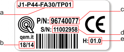
-
a - Ordering Code
-
b - Week made: indicates the week and year of manufacture
-
c - Part number: unique code that identifies an ordering code
-
d - Serial number: product serial number, different for individual product
-
e - Hardware release: version of hardware release
1.1.2 Ordering Code
Model Features J1 - P44 - FA - 10 / TP01 
TP00 = Keypad code (TP00 = panel with resistive, logo and custom function keys;
TP01 = panel with resistive touch-screen, logo and QEM standard function keys10 = Firmware version (00 = not installed) F = Technology level
A = Hardware versionP = Basic keypad (only function keys)
4 = 8” LCD graphic display, TFT-256 COLORI-800x600px; front panel dimensions (240x192mm); keypad 6 keys + 10 led; housing to DIN 43700;
4 = Firmware-hardware correspondenceJ1 = „HMI+PLC“ Qmove family 1.1.3 Hardware Versions
These are hardware versions currently available:
Hardware versions A B C E F H I Y Base
cardUSER PORT (RS232-422-485) - - - - - 1 - 1 AUX PORT (RS485) 1 1 1 1 1 1 1 1 CAN1 PORT 1 1 1 1 1 1 1 1 CAN2 PORT 1) - - - - - - - - ETHERNET PORT 1 1 1 1 1 1 1 1 USB PORT 1 1 1 1 1 1 1 1 Standard digital inputs 16 16 16 16 16 16 16 16 16bit selectable analog input(0-10V, 0-20mA, potentiometer, thermocouples, PT100) 2 2 2 2 2 2 2 2 200kHz two-way count inputs, ABZs(24V-PP, 5V-LD) - 2 42) 2 43) 44) 45) 46) SSI counts - - - - - - - 2 Protected digital outputs 16 16 16 16 16 16 16 16 Stepper outputs - - - - - - - 2 +/-10V, 16bit analog outputs - 2 4 2 4 4 4 4 Card software code declared in Base card 1QM4F Specialist
cardDigital input - - - 16 16 - 16 - Selectable 16bit analog input(0-10V, 0-20mA, potent., thermoc., PT100) - - - - 2 - 2 - Protected digital outputs - - - 16 16 - 16 - +/-10V, 16bit analog outputs - - - - - - 2 - 200kHz two-way count inputs, ABZs(24V-PP, 5V-LD) - - - - - - 2 - Card software code declared as specialist card - - - 1MG2F 1MG2F - 1MG2F - 1.1.4 Expansion Board Manuals
1.1.5 Firmware versions
Version Description 10 Fully programmable with PLC functions 20 Fully programmable with PLC and Motion control functions 30 Fully programmable with PLC, Motion control, Camming and Interpolation functions For more details about the firmware, consult Devices enabled in the controllers.
1.2 Product Configuration
1.2.1 Front Panel
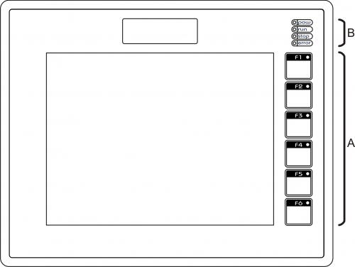
A) Function keys and led's
B) System led's
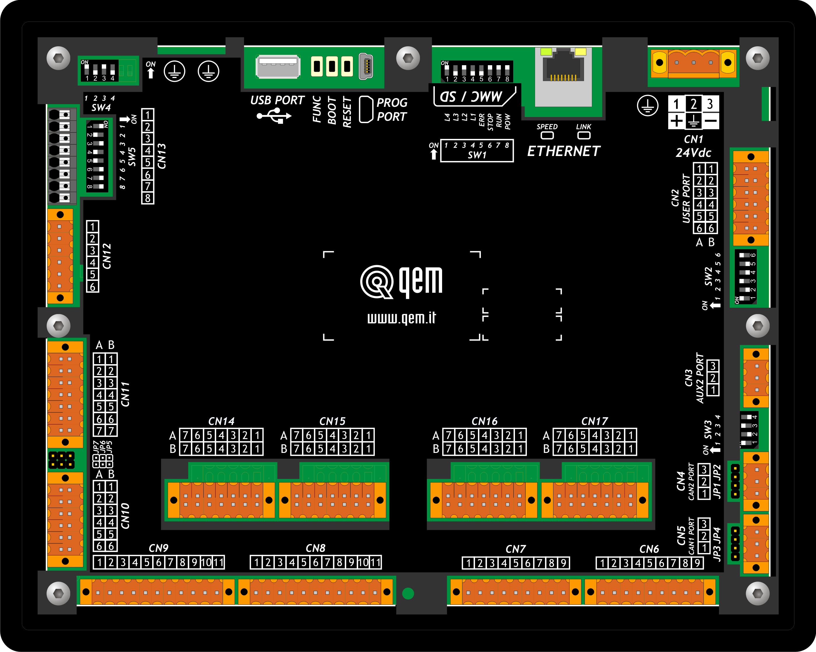
1.2.2 Back terminal blocks
J1-P44-F composed of a „base“ card and an „expansion“ card.
-
a = Base card
-
b = Expansion card
2. Technical features
2.1 General Features
Weight (full hardware) 1.2Kg Housing Sheet metal Front panel Alluminium Outer Frame Self-extinguishing Noryl Display 8'' LCD TFT 256 colours - 800*600px Touch screen 4-wire Resistive Display dimensions 162.0 x 121.5mm / 8„ User led's 6 System led's 4 Function keys 6 System keys 3 Operating temperature 0 ÷ 50°C Transport and storage temperature -25 ÷ +70 °C Relative humidity 90% condensate free Altitude 0 - 2000m a.s.l. Front protection rating IP64 2.2 CPU (F level technology)
RISC microprocessor (32 bit) Work frequency 200MHz RAM 32MB Flash 16MB 2.3 Dimensions

Lengths in mm 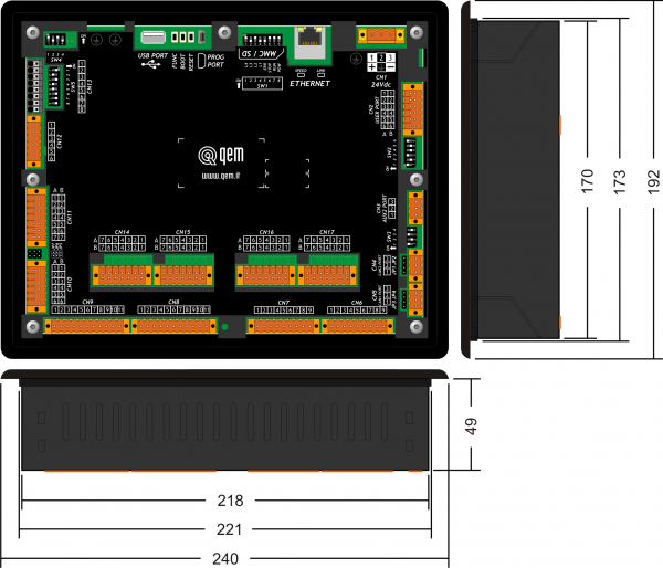
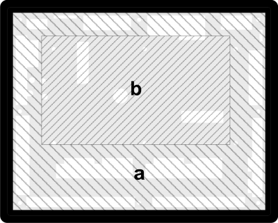
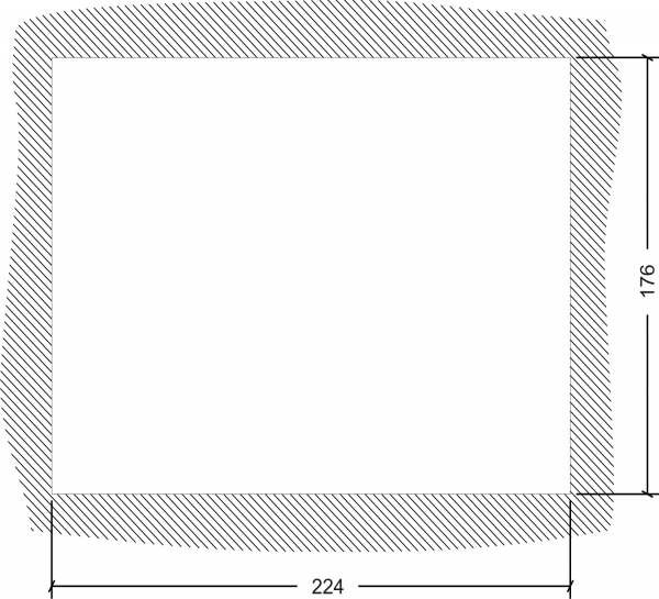
2.4 Hole template
2.5 Installation
Fit the controller in the hole.

Apply the brackets.
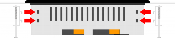

Before fixing the controller, check it is mounted firmly in the hole and the gasket under the frame makes a good seal. No liquids must enter and the frame must not deform. Screw the controller in place.
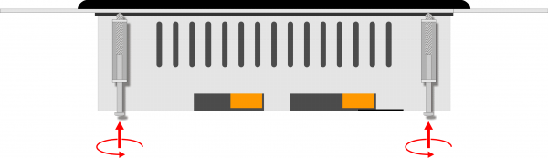
Warning: after putting the pin of fixing, do only half rotation to not tear the frame! 3. Base card wiring
For details about cable sections and connectors, see application note AN021 .
The electrical features are given in paragraph Electrical features.
The connection examples are provided in paragraph Connection examples
3.1 Power supply

The cabling must be carried out by specialist personnel and fitted with suitable anti-static precautions.
Before handling the controller, disconnect the power and all parts connected to it.
To guarantee compliance with EC regulations, the power supply must have a galvanic isolation of at least 1500Vac..
Power supply 24 Vdc Voltage range 22 - 27 Vdc Max. absorption 10W Connector
CN1 Terminal Symbol Description 

1 
DC power positive 2 GROUND Gnd-PE (signals) 3 
DC power 0V Connection examples
Use an isolated power unit with 24Vdc +/-5% output conform to EN60950-1. .
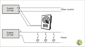
Use two separate power units: one for the control circuit and one for the power circuit 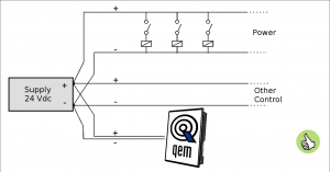
For a single power unit, use two separate lines: one for the control and one for the power 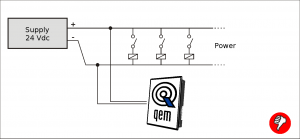
DO NOT use the same lines for the power circuit and the controller 3.2 Serial Port Connections
3.2.1 PROG PORT (USB mini-B)
3.2.2 USER PORT
USER PORT connector
CN2 Terminal RS232 RS422 RS485 Description 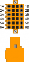
1A - - A Terminal A - RS485 2A - - B Terminal B - RS485 3A 0V 0V 0V USER PORT common 4A 0V 0V 0V USER PORT common 5A TX - - Terminal TX - RS232 6A Ground 1B - RX - Terminal RX - RS422 2B - RXN - Terminal RX N - RS422 3B - TX - Terminal TX - RS422 4B - TXN - Terminal TX N - RS422 5B RX - - Terminal RX - RS232 6B Ground USER PORT electrical standard setting
3.2.3 AUX PORT
Connector
CN3 Terminal Symbol Description 
1 0V RS485 serial common 2 B Terminal RS485 B 3 A Terminal RS485 A Setup of AUX2 PORT polarisation and termination resistances
3.2.3.1 CANbus PORT
Connector
CN5
CAN1 PORTTerminal Symbol Description 1 0V CAN common 2 CAN L Terminal CAN L 3 CAN H Terminal CAN H Termination resistor setting
Name
jumperSetting of DIP Function JP3 JP4

JP3 INSERTED Termination CAN active JP4 Connector
CN4
CAN2 PORTTerminal Symbol Description 1 0V CAN common 2 CAN L Terminal CAN L 3 CAN H Terminal CAN H Termination resistor setting
Name
jumperSetting of DIP Function JP1 JP2
JP1 INSERTED Termination CAN active JP2 3.2.4 ETHERNET port
ETHERNET PORT Description 
Connector RJ45.
LED:
* LINK: green led = cable connected (led on signals the cable is connected to both ends)
* DATA: yellow led = data transmission (flashing led signals data transmission)3.2.5 MMC/SD
 Memory card slot (marked by an arrow)
3.2.6 USB

3.3 Digital Inputs
3.3.1 16 Digital inputs, PNP
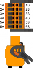
CN7 Terminal Symbol Description Addres 
1 0V Common for digital inputs 2 I1 Input I1 2.INP01 3 I2 Input I2 2.INP02 4 I3 Input I3 2.INP03 5 I4 Input I4 2.INP04 6 I5 Input I5 2.INP05 7 I6 Input I6 2.INP06 8 I7 Input I7 2.INP07 9 I8 Input I8 2.INP08 .
CN6 Terminal Symbol Description Address 1 0V Common for digital inputs 2 I9 Input I9 2.INP09 3 I10 Input I10 2.INP10 4 I11 Input I11 2.INP11 5 I12 Input I12 2.INP12 6 I13 Input I13 2.INP13 7 I14 Input I14 2.INP14 8 I15 Input I15 2.INP15 9 I16 Input I16 2.INP16 3.3.2 4 two-way count inputs, 200KHz
CN14 Terminal Symbol Description Address 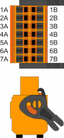
1A Output + 24V dc1) 2A PHA1 Phase A Count 1
PNP / Push-Pull2)2.INP17 2.CNT01 3A PHB1 Phase B 2.INP18 4A Z1 Z 1.INT01 5A 0V Common for count inputs 6A 0V 7A 0V 1B Output + 24V dc3) 2B PHA1+ + PHA Count 1
Line Driver2.INP17 2.CNT01 3B PHB1+ + PHB 2.INP18 4B Z1+ + Z 1.INT01 5B PHA1- - PHA 6B PHB1- - PHB 7B Z1- - Z
2) PNP/Push-Pull type count input configuration:
Terminal 5B: connect to terminal 5A
Terminal 6B: connect to terminal 6A
Terminal 7B: connect to terminal 7ACN15 Terminal Symbol Description Address
1A Output + 24V dc1) 2A PHA2 Phase A Count 2
PNP / Push-Pull2)2.INP19 2.CNT02 3A PHB2 Phase B 2.INP20 4A Z2 Z 1.INT02 5A 0V Common for count inputs 6A 0V 7A 0V 1B Output + 24V dc3) 2B PHA2+ + PHA Count 2
Line Driver2.INP19 2.CNT02 3B PHB2+ + PHB 2.INP20 4B Z2+ + Z 1.INT02 5B PHA2- - PHA 6B PHB2- - PHB 7B Z2- - Z
2) PNP/Push-Pull type count input configuration:
Terminal 5B: connect to terminal 5A
Terminal 6B: connect to terminal 6A
Terminal 7B: connect to terminal 7ACN16 Terminal Symbol Description Address
1A Output + 24V dc1) 2A PHA3 Phase A Count 3
PNP / Push-Pull2)2.INP21 2.CNT03 3A PHB3 Phase B 2.INP22 4A Z3 Z 1.INT03 FREQ13) 5A 0V Common for count inputs 6A 0V 7A 0V 1B Output + 24V dc4) 2B PHA3+ + PHA Count 3
Line Driver2.INP21 2.CNT03 3B PHB3+ + PHB 2.INP22 4B Z3+ + Z 1.INT03 FREQ15) 5B PHA3- - PHA 6B PHB3- - PHB 7B Z3- - Z
2) PNP/Push-Pull type count input configuration:
Terminal 5B: connect to terminal 5A
Terminal 6B: connect to terminal 6A
Terminal 7B: connect to terminal 7ACN17 Terminal Symbol Description Address
1A Output + 24V dc1) 2A PHA4 Phase A Count 4
PNP / Push-Pull2)2.INP23 2.CNT04 3A PHB4 Phase B 2.INP24 4A Z4 Z 1.INT04 FREQ23) 5A 0V Common for count inputs 6A 0V 7A 0V 1B Output + 24V dc4) 2B PHA4+ + PHA Count 4
Line Driver2.INP23 2.CNT04 3B PHB4+ + PHB 2.INP24 4B Z4+ + Z 1.INT04 FREQ25) 5B PHA4- - PHA 6B PHB4- - PHB 7B Z4- - Z
2) PNP/Push-Pull type count input configuration:
Terminal 5B: connect to terminal 5A
Terminal 6B: connect to terminal 6A
Terminal 7B: connect to terminal 7A3.3.3 2 SSI absolute counters
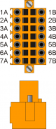
CN11 Terminal Symbol Description Address 1A Internal bridge 1A-2A-1B-2B 2A 3A DATA1+ DATA in SSI1 1 4A DATA1- 5A CLOCK1+ CLOCK out SSI1 6A CLOCK1- 7A 0V Common for count inputs 1B Internal bridge 1A-2A-1B-2B 2B 3B DATA2+ DATA in SSI2 2 4B DATA2- 5B CLOCK2+ CLOCK out SSI1 6B CLOCK2- 7B 0V Common for count inputs 3.4 Analog inputs
3.4.1 2 multistandard analog input
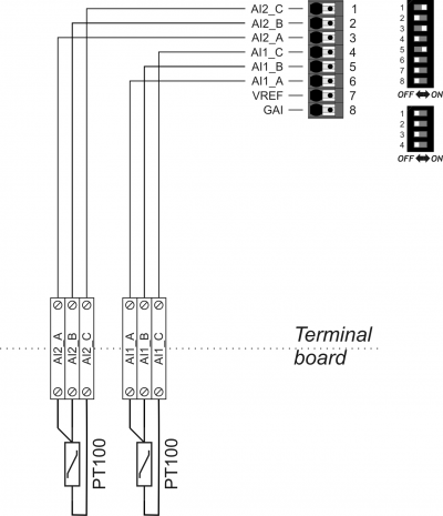
Connector
Analog inputs setting
Num.
DipAnalog input 1 Analog input 2 PT100 Thermocouple Pot. 0-10V 0-20mA PT100 Thermocouple Pot. 0-10V 0-20mA SW5

1 ON X OFF OFF OFF X X X X X 2 OFF X ON ON ON X X X X X 3 X X X X X ON X OFF OFF OFF 4 X X X X X OFF X ON ON ON 5 ON ON OFF OFF OFF X X X X X 6 OFF OFF ON ON ON X X X X X 7 OFF ON X X X X X X X X 8 X X X X X OFF ON X X X SW4

1 X X X X X X X OFF OFF ON 2 X X X X X X X OFF ON OFF 3 X X OFF OFF ON X X X X X 4 X X OFF ON OFF X X X X X X = irrelevant setting
Pot. = potentiometric type input3.5 Digital outputs
3.5.1 16 protected outputs
CN9 Terminal Symbol Description Address 
1 V+ Outputs power input O1÷O4 (12÷28V dc) 2 O1 Digital output 1 2.OUT01 3 O2 Digital output 2 2.OUT02 4 O3 Digital output 3 2.OUT03 5 O4 Digital output 4 2.OUT04 6 V+ Outputs power input O5÷O8(12÷28V dc) 7 O5 Digital output 5 2.OUT05 8 O6 Digital output 6 2.OUT06 9 O7 Digital output 7 2.OUT07 10 O8 Digital output 8 2.OUT08 11 V- Outputs power in (0V dc) .
CN8 Terminal Symbol Description Address 1 V+ Outputs power input O9÷O12(12÷28V dc) 2 O9 Digital output 9 2.OUT09 3 O10 Digital output 10 2.OUT10 4 O11 Digital output 11 2.OUT11 5 O12 Digital output 12 2.OUT12 6 V+ Outputs power input O13÷O16(12÷28V dc) 7 O13 Digital output 13 2.OUT13 8 O14 Digital output 14 2.OUT14 9 O15 Digital output 15 2.OUT15 10 O16 Digital output 16 2.OUT16 11 V- Outputs power in (0V dc) 3.5.2 2 STEP-DIRECTION outputs
Connector
CN10 Terminal Symbol Description Address 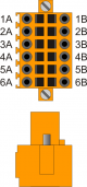
1A VD1 Internal bridge 1A -1B 2A DIR1+ Output DIRECTION 1 Push-Pull Line Driver 2.PULSE01 3A STEP1+ Output STEP 1 4A DIR2+ Output DIRECTION 2 2.PULSE02 5A STEP2+ Output STEP 2 6A 0V Common for stepper outputs 1B VD1 Internal bridge 1A -1B 2B DIR1- Complementary output DIRECTION 1 Complementary outputs for use in drives with Line-Driver inputs 3B STEP1- Complementary output STEP 1 4B DIR2- Complementary output DIRECTION 2 5B STEP2- Complementary output STEP 2 6B 0V Common for stepper outputs Outputs STEP-DIRECTION voltage setting
By placing one of several jumpers JP5, JP6 and JP7, you can choose Nominal Operating Voltage of STEP and DIRECTION outputs.
Must be inserted only one jumper at a time
If you select one of the two voltage 5V (JP7) or 12V (JP5) terminals 1A and 1B must remain disconnected.
jumper
nameSetting Nominal voltage 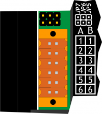
JP5 INSERTED 12V (Voltage supplied by the instrument)

JP6 INSERTED VD1 (Voltage to be supplied to the terminals 1A or 1B) JP7 INSERTED 5V (Voltage supplied by the instrument) 3.6 Analog outputs
3.6.1 4 analog outputs +/-10V, 16bit
CN12 Terminal Symbol Description Address 
1 GAO Common for analog outputs 2 AO1 Analog output 1 2.AN01 3 AO2 Analog output 2 2.AN02 4 GAO Common for analog outputs 5 AO3 Analog output 3 2.AN03 6 AO4 Analog output 4 2.AN04 4. Electrical Features
The electrical features of the hardware are given below.
The maximum and minimum frequencies, and real acquisition times, may depend on eventual additional software filters.4.1 PROG PORT (USB mini-B)
The USB mini-B connector does not support USB electrical standards, it can only be used with an interface IQ009 or IQ013. It is used for the transfer and debugging of the application program in the CPU.
Electrical standard TTL (Use serial interface IQ009 or IQ013) Communication speed Min. 9.6 Kbaud - max 115200 Kbaud
settable by dip1 and 2 of the switch SW1Insulation None .

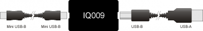

Connection between Qmove+ e PC using the accessory IQ009 .
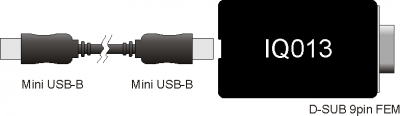
Connection between Qmove+ and a device fitted with a RS232 serial port (e.g. a MODEM), using the interface IQ013 4.2 RS232
Communication speed 4800, 9600, 19200, 38400, 57600, 115200 baud Communication mode Full duplex Operating mode Referred to 0V Max. number of devices connected on the line 1 Max. cable length 15 m Input impedence > 3 Kohm Short-circuit current limit 7 mA 

4.3 RS422
Communication speed 4800, 9600, 19200, 38400, 57600, 115200 baud Communication mode Full duplex Operating mode Differential Max. number of devices connected on the line 1 Max. cable length 1200 m Input impedence > 12 Kohm Short-circuit current limit 35 mA 


4.4 RS485
To activate the internal termination resistance see paragraph Setup of USER PORT electric standard, Setup of AUX1 PORT electric standard or Setup of AUX2 PORT polarization and termination resistances .
Communication speed 4800 baud (only if used with SERCOM and/or MODBUS device),
9600 baud, 19200 baud, 38400 baud, 57600 baudCommunication mode Half duplex Operating mode Differential Max. number of devices connected on the line 32 Max. cable length 1200 m Input impedence > 12 Kohm Short-circuit current limit 35 mA 

4.5 CAN BUS
To activate the internal termination resistance see paragraph Setup Termination resistances
.
Communication speed 125, 250, 500, 1000 Kbit/s Max. number of Drivers/Receivers on the line 100 Max. cable lengths 500m @ 125Kbit/s, 250m @ 250Kbit/s, 100m @ 500Kbit/s, 25m @ 1000Kbit/s Input impedence >15Kohm Short-circuit current limit 45mA 


CAN BUS connection examples.
Caution:
Close DIP's JP1 and JP2 and insert the termination resistances (RL, RH) on the last device of the chain.4.6 ETHERNET
Ethernet Interface 10/100 Base T (IEEE 802.3) on RJ45 connector.
Connection between Qmove + and PC:
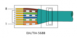
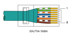
Qmove+ Cross-over cable EIA/TIA-568A/B PC 4.7 MMC/SD
Type of Memory Card to use MMC, SD and SDHC up to 8GB
For proper operation it is necessary that the device conforms to the standards set by „SD Association“ (www.sdcard.org) or „Multi Media Card Association“ (www.mmca.org)..
To use the Memory Cards they must first be formatted with FAT16 or FAT32 file system. 4.8 USB
Max output current 500mA 4.9 Standard digital inputs
Type of polarisation PNP Min. acquisition time (hardware) 3ms Isolation 1000Vrms Rated operating voltage 24Vdc Voltage of logic state 0 0-2 V Voltage of logic state 1 10.5 - 26.5 V Internal voltage drop 5V Input resistance (Ri) 2700Ω Sink current 2mA ÷ 8mA1)
1) CAUTION: If the device connected to the inputs needs a higher minimum current, inputs may not work properly.
4.10 Two-way count inputs, 200KHz
The values given in the table refer to input signals A, B and Z.
The max. frequency given in the table refers to A and B phase signals with a DutyCycle = 50%
With count frequencies over 50KHz the use of Line-Driver type encoders is recommended.Type of polarisation PNP/PP Max frequency 200KHz Min. acquisition time 5µs Insulation 1000Vrms Rated operating voltage 24Vdc Voltage of logic status 0 0 - 2 V Voltage of logic status 1 10.5 - 26.5 V Internal voltage drop 1.2V Input resistance 3100Ω Line-Driver
Type of polarisation Line-Driver Max. frequency 200KHz Min. acquisition time 5µs Insulation 1000Vrms Rated operating voltage (PHx+ ? PHx-) 5Vdc Voltage of logic status 0 (PHx+ ? PHx-) 0-1.5 V Voltage of logic status 1 (PHx+ ? PHx-) 2-5 V Internal voltage drop 1.2V Input restistance 150Ω 
4.11 SSI absolute counts
Frequency 320KHz Operation mode Differential Input impedance >= 12KO Short circuit current limit >= 35mA 
4.12 Analog inputs
4.12.1 Conversion time
The electrical features depend on the type of input, configurable via DIP switch.
The conversion times from analog to digital depend on the configuration according to the table:
Analog Input Configuration Conversion time
per channelInput 1 Input 2 DC1) - 4.6 ms - DC2) 4.6 ms DC3) DC4) 9.3 ms DC5) TC 9.3 ms DC6) PT100 79.1 ms TC - 9.3 ms - TC 9.3 ms TC DC7) 9.3 ms TC TC 9.3 ms TC PT100 83.8 ms PT100 - 74.5 ms - PT100 74.5 ms PT100 DC8) 79.1 ms PT100 TC 79.1 ms PT100 PT100 79.1 ms 4.12.2 Amperometric analog inputs, 0-20mA
Connection type Amperometric
(0-20 mA)Resolution 12bit/16bit1) Input resistance 125Ω Value of damage 25 mA Max. Linearity error + 0,1% Vfs Max. Offset error + 0,1% Vfs S.n. 71 dB Conversion time It depends on the configuration of the analog input.
See section Conversion times if present 2)Isolation 1000 Vrms
1) It depends on the Hardware versions2) The sampling time of the device must be equal or higher than the conversion time
4.12.3 Potentiometric analog inputs
Connection type Potentiometric 1KΩ÷20KΩ Resolution 12bit/16bit1) Reference voltage output 2,5Vdc Max output current from reference 10mA Input resistance 10MΩ Max. Linearity error + 0,1% Vfs Max. Offset error + 0,1% Vfs S.n. 71 dB Conversion time It depends on the configuration of the analog input.
See section Conversion times if present 2)Isolation 1000 Vrms
1) It depend on the Hardware versions2) The sampling time of the device must be equal or higher than the conversion time
4.12.4 Voltmetric analog inputs
Connection type Voltmetrico
0÷10VResolution 12bit/16bit1) Input resistance (Rin) 40KΩ Value of damage 20V Max. Linearity error + 0,1% Vfs Max. Offset error + 0,1% Vfs S.n. 71 dB Conversion time It depends on the configuration of the analog input.
See section Conversion times if present 2)Isolation 1000 Vrms
1) It depends on the Hardware versions2) The sampling time of the device must be equal or higher than the conversion time
4.12.5 PT100 analog inputs
Sensor type
collegabilePT100 3 wire 1) Measure type Resistance 2) Resolution 15 bit (32767 corresponds to 250.00 O) Input resistance (Rin) 15 MO Measuring current 1 mA Value of damage 10V Accuracy of resistance measurement ± 0,04% Conversion time It depends on the configuration of the analog input.
See section Conversion times if present 3)Isolation 1000 Vrms 4.12.6 Termocouples analog inputs
Sensor type Thermocouple type J,K,R,S,B,N,T,E 1) Type of measure Differential voltage Resolution 16 bit Measuring range ±156.25 mV Measure for cold junction compensation Integrated Input resistance (Rin) 15 MO Value of damage 30V Measurement accuracy ± 0,2% (excluding cold junction compensation) Conversion time It depends on the configuration of the analog input.
See section Conversion times if present 2)Isolation 1000 Vrms 4.13 Protected Digital Outputs
Switchable load Dc (PNP) Max. operating voltage 28V Insulation 1000Vpp Max. internal voltage drop 600mV Max internal resistance @ON 90mΩ Max. protection current 12A Max. operating current 2A Max. current @OFF 5µA Max switching time from ON to OFF 270µs Max switching time from OFF to ON 250µs 
4.14 STEP-DIRECTION outputs
Type of polarisation Push-Pull / Line-Driver Max output frequency 200KHz Insulation 1000Vpp Max. operating current 20mA Max. voltage 24Vdc1)
1) Selectable via jumpers: 5V e 12V supplied by the instrument, 24V supply from outside to the terminal VDx
4.15 Analog outputs
Type of connection Common mode Insulation 1000Vrms Voltage range (minimum no load) -9.8V - +9.8V Max. offset variation depending on temperature* +/- 5mV Resolution 16bit Max. current 1mA Output variation depending on load 100 µV/mA Output resistence 249Ω 
5. Connection examples
5.1 CANbus

On the first (1) and on the last (3) device of the chain, the termination resistances must be inserted.
The cable shoes must be connected to ground by the fastons provided on the metal body..
To activate the internal termination resistance see paragraph Setup of CAN1 and CAN2 PORT Termination resistances
Caution: close the DIP JP1 and JP2 and insert the terminating resistors (RL, RH) on the last device in the chain. 5.2 Digital inputs

5.3 Line Driver counts

5.4 PNP / Push Pull counts

5.5 SSI absolute counts

5.6 Analog inputs
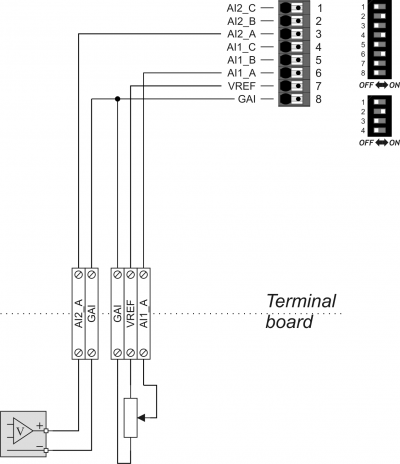
5.6.1 1 potentiometric e 2 voltmetric
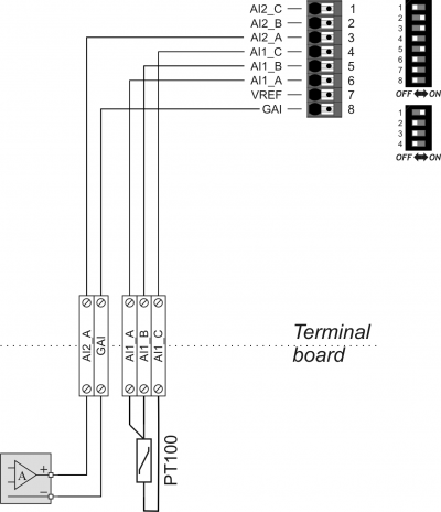
5.6.2 1 PT100 e 2 amperometric
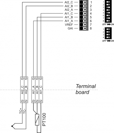
5.6.3 1 PT100 and 2 termocouples
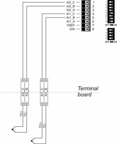
5.6.4 1 e 2 for termocouples
5.6.5 1 and 2 PT100
5.7 Protected digital outputs

5.8 STEP-DIRECTION outputs

5.9 Analog outputs

6. Settings, procedures and signals

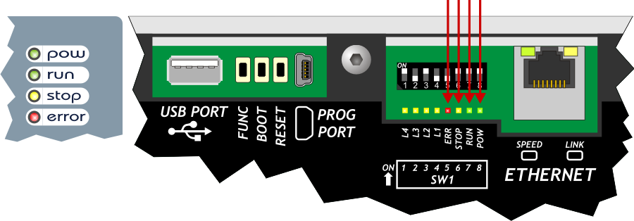
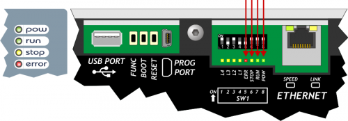
6.1 PROG PORT, USER PORT and CAN PORT baud-rate selector
SW1 Dip DIP settings Function 
1 OFF Baud-rate 57600 Select PROG PORT transmission speed ON Baud-rate 115200 2 OFF Baud-rate 57600 Select USER PORT transmission speed ON Baud-rate 115200 3 OFF Can also be used by SERCOM and MODBUS devices Select PROG PORT functioning mode ON Cannot be used by SERCOM and MODBUS devices 4 OFF ON OFF ON CANbus baud-rate selector (CanOpen)1) 5 OFF OFF ON ON Baud-rate
125KB/SBaud-rate
250KB/SBaud-rate
500KB/SBaud-rate
1MB/S6 OFF IQ009 connection Mini USB 5Vdc supply2) ON IQ021 connection 7 Not used 8 OFF PROG PORT normal Select the USER PORT as PROG PORT3) ON PROG PORT on USER PORT connector
1) Valid if the declaration of the CANopen device is set the speed to 02) If enabled, on the mini USB connector of the PROG POR, 5Vdc are available for the IQ021 Bluetooth Interface power supply.3) It is possible to use the USER PORT connector as PROG PORT with RS232 electric standard, doing this the mini-USB connector of the PROG PORT is disconnected (Setting USER PORT electric standard). For this function mode also set dip 6 of SW2 to OFF.6.2 Led
The system leds „pow, run, stop, err“ are found on the front panel and on the rear of controllers with display and only on the top of controllers without display.
The user leds „L1, L2, L3 e L4“ are found on the rear:

“System Leds” Signals
Leggend:
 Led ON
 Led OFF
 Led Blinking
Led Colour Status Description pow Green 
Power on Only this led on, signals the CPU reset status run Green CPU in RUN status 
CPU in READY status stop Yellow With pow on, signals the STOP status of the CPU
With pow off, signals the BOOT status of the CPUerr Red With pow off, signals a hardware error. See paragraph Hardware Error codes
With pow blinking, the flash rate gives the type of error. See paragraph err led signalsErr led signals
N.
flashesError Description Recommended action 1 Bus error Bus configuration different to application software. Check the correspondence between the QMOVE application (BUS section of configuration unit) and the product configurations (cards mounted in BUS). 2 CheckSum Error Negative outcome on the integrity control of retentive variables . (see Reset Error Checksum) Restore the machine data from a backup (.DAT file) or cancel the error with in system functions and enter the values manually. 3 Index Out of Bound An array index is pointing on an inexistent element Open a unit editor in Qview development environment and use the „Edit→Go to PC“ command to find the program line that is cause of the error. In general the index value has a value <1 or >array dimension. 4 Program Over Range The program selection index in the DATAGROUP has attempted to access an inexistent program. With the Qview development environment open the editor of a unit and user the „Edit→Go to PC“ command to highlight the program line that has caused the error. In general the value used as index is lower than 1 or over the array dimension. 5 Step Over Range The step selection index in the DATAGROUP has attempted to access an inexistent step. With the Qview development environment open the editor of a unit and user the „Edit→Go to PC“ command to highlight the program line that has caused the error. In general the value used as index is lower than 1 or over the array dimension. 6 Division By Zero The denominator of a division operation of the application program has a zero value. With the Qview development environment open the editor of a unit and user the „Edit→Go to PC“ command to highlight the program line that has caused the error. 7 Syntax Error The application program has an invalid instruction This error may appear because the program counter has met the QCL END instruction. 8 Watch Dog Error A CAN module does not function correctly, or a specialist card has a hardware problem With the Qview development environment open the „Monitor→Bus“ panel and the righthand column called „Watchdog Bus“ indicates the card that caused the problem. 9 Stack Error The applciation program has used all permitted levels of calls to subroutines With the Qview software environment open the editor of a unit and use the „Edit→Go to PC“ command to highlight the program line that caused the error. Analyse the unit execution flow, the call to subroutines nestings have a limit, over which this error is generated. Hardware error codes
During the startup sequence, if a malfunction of any peripheral is detected, the system blocks and the error is signaled by the flashing led
err while the other system led's remain off.
The number of flashes indicates the type of error according to the following table :
Number of flashes Error 1 Display 2 FPGA 3 Media 4 Bootloader 5 FW 6 Bus 7 Signal not active 8 Signal not active 9 Exception .
Each of these signals indicates a serious error situation. The product must be sent to the QEM aftersales service. “User Led” signal
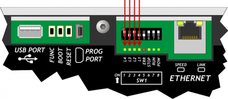
Led Colour Description L1Yellow Programmable in the application program by the QMOVE system variable:sys003 and used by the system functions L2 L3 L46.3 Keys
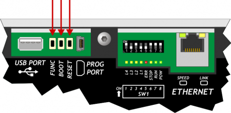
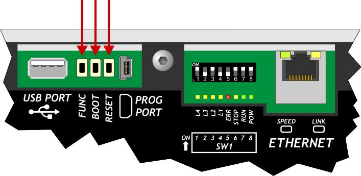
Name Description  FUNC
FUNCPress on startup of the controller to access the System functions BOOTPress on startup of the controller to set the CPU in Boot status and then access the firmware update functions RESETReset CPU. the system is restarted restoring the initial conditions (after a startup ) 7. System functions
IMPORTANT: The use of these procedures could represent a risk (e.g. see deletion of application), therefore it is highly recommended that they are performed by qualified experts. The system functions are specific procedures that allow the user to perform various operations, e.g. the configuration/calibration of peripherals, data and application save/restore on/from removable mass memory, deletion of the application and management of the mass storage.
Controllers with display have some system functions that are only accessible by password and if access attempts are made the „Function is locked“ message is given.7.1 System functions
All the system functions are listed below.
If the „PWD“ column shows 'Y', this means that the function requires a system password (default: „123“).Funzioni di sistema
n. Led ON System Function PWD Description 1 L1 01 - Reset Error Checksum - Reset error checksum.
N.B.: if the checksum error is present, the ledL1 flashes 2 L2 02 - Copy all files DEVICE → NAND - Copy all files from selected DEVICE to NAND Flash memory 3 L1
L2 03 - Copy all files NAND → DEVICE - Copy all files from NAND Flash to selected DEVICE 4 L3 04 - Application delete Y Delete the application 5 L1
L3 05 - Application upload from DEVICE Y Upload the application from selected DEVICE 6 L2
L3 06 - System Settings - Adjust the system clock and select the DEVICE in use 7 L1
L2
L3 07 - Downl. retentive data to DEVICE - Save the retentive data on selected DEVICE 8 L4 08 - Set NEW Password Y Set a new password to access the „locked“ system functions 9 L1
L4 09 - Remove all files from NAND Flash Y Cancel all files stored on the NAND Flash memory 10 L2
L4 10 - Show NAND Flash files - List the files stored on the NAND Flash memory 11 L1
L2
L4 11 - Touch Calibration - Run the calibration procedure of the Touch Screen, if present 12 L3
L4 12 - Set Ethernet communic. parameter - Run the setup procedure for the Ethernet communication parameters (IP address,…, etc.) 13 L1
L3
L4 13 - Backup to NAND - Run the backup of the QCL application, data and HMI application on NAND memory 14 L2
L3
L4 14 - Restore from NAND Y Run the restore of the QCL application, data and HMI application from NAND memory NB: To exit system functions press the keep the F1 key or FUNC button for at least two seconds.
8. Available accessories
-
-


 A and B cables are connected to the same head of the PT100 wire and have the same colors.