Indice
J1-P51-Fx - Hardware manual

Release
| Document release | Description | Notes | Date |
|---|---|---|---|
| 01 | New manual | / | 03/12/2012 |
The controller has been designed for industral environments in conformity to EC directive 2004/108/CE.
-
EN 61000-6-4: Electromagnetic compatibility - Generic standard on emission for industrial environments
-
EN55011 Class A: Limits and measurement methods
-
EN 61000-6-2: Electromagnetic compatibility - Generic standard on immunity for industrial environments
-
EN 61000-4-2: Electromagnetic compatibility - Electrostatic discharge immunity
-
EN 61000-4-3: Immunity to radiated, radio-frequency electromagnetic field
-
EN 61000-4-4: Electrical fast transients
-
EN 61000-4-5: Surge immunity
-
EN 61000-4-6: Conducted disturbance induced by radio-frequency
-
Moreover the product is conform to the following standards:
-
EN 60529: Housing protection rating IP64
-
EN 60068-2-1: Environmental testing: Cold
-
EN 60068-2-2: Environmental testing: Dry heat
-
EN 60068-2-14: Environmental testing: Change of temperature
-
EN 60068-2-30: Environmental testing: Cyclic damp heat
-
EN 60068-2-6: Environmental testing: Sinusoidal vibration
-
EN 60068-2-27: Environmental testing: Shock vibration
-
EN 60068-2-64: Environmental testing: Random vibration
-
1. Information
Product Identification
The Ordering Code provides the exact product characteristics. Make sure that the product characteristics meet your requirements.
Product Label

-
a - Ordering Code
-
b - Week made: indicates the week and year of manufacture
-
c - Part number: unique code that identifies an ordering code
-
d - Serial number: product serial number, different for individual product
-
e - Hardware release: version of hardware release
Ordering Code
Model Characteristics J1 - P51 - FA - 30 / TP01 -
J1 = Qmove “HMI+PLC” Qmove family
-
P = Basic keypad (only function keys)
-
5 = 10.4” LCD graphic display, TFT-256 COLOURS-800x600px; front panel dimensions (216x287mm); keypad 6 keys + 10 led; housing to DIN 43700;
-
1 = Firmware-hardware correspondence
-
F = Technology level
-
A = Hardware version
-
30 = Firmware version (00 = not installed)
-
TP01 = Keypad code (TP00 = panel with resistive, logo and custom function keys; TP01 = panel with resistive touch-screen, logo and QEM standard function keys
Hardware Versions
There are currently 6 hardware versions available:
Hardware Versions A B C D E W SLOT 2
(Base Card)USER PORT (RS232, RS422, RS485) 1 1 1 1 1 1 AUX1 PORT (RS232, RS422, RS485) - - - - - - AUX2 PORT (RS485) - - - - - - CAN1 PORT 1 1 1 1 1 1 CAN2 PORT - - - - - - ETHERNET PORT - 1 1 1 1 1 USB PORT1) - - - - - - SLOT 3
(Specialist
card)Standard digital inputs - 32 32 32 32 - Fast digital inputs 2) - 2 2 2 2 - 12bit analog inputs - 4 4 4 4 - 16bit analog inputs - - - - - - PT100 inputs 3) - - - - - - Thermocouple inputs 4) - - - - - - 20kHz two-way count inputs, ABZ
(24V-PP, 5V-LD)- - - - - - 200kHz two-way count inputs, ABZ
(24V-PP, 5V-LD)- 2 4 6 8 - Protected digital outputs - 32 32 32 32 - Digital relay outputs - - - - - - 0-10V, 12bit analog outputs - - - - - - +/-10V, 16bit analog outputs - 2 4 6 8 - Stepper outputs - - - - - - Qem remote keypad connector 5) - - - - - - Card software code
declared in SLOT 3- 1MG8F 1MG8F 1MG8F 1MG8F - Firmware Versions
Version Description 10 Fully programmable with PLC functions 20 Fully programmable with PLC and Motion control functions 30 Fully programmable with PLC, Motion control, Camming and Interpolation functions For more details about the firmware, consult Devices enabled in the controllers.
1.1 Product Configuration
Front Panel

A) Function keys and led's
B) System led'sBack terminal blocks
J1-P51-F has a specialist card in slot 3.

Slot Description Slot Supply Power connector on base card Slot 2 Base card Slot 3 Expansion card 2. Technical Features
General Features
Weight (full hardware) 2Kg Housing Sheet metal Front panel Aluminium Outer Frame Self-extinguishing Noryl Display 10.4” LCD TFT-256 COLOURS-800 x 600px Touch screen 4-wire Resistive Display dimensions/diagonal 211.2 x 158.4mm/ 10.4“ User led's 6 System led's 4 on front panel, 8 on back Function keys 6 System keys 3 Operating temperature 0 - 50°C Relative humidity 90% condensate free Altitude 0 - 2000m a.s.l. Transport and storage temperature -25 - +70 °C Front protection rating IP64 CPU (F level technology)
RISC microprocessor (32 bit) Work frequency 200MHz RAM 16MB Flash 8MB For more information on the memory consult Memories used
Dimensions
Lengths in mm.

Hole template

Fit the controller in the hole.

Apply the brackets.
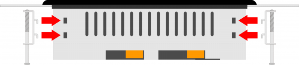

Before fixing the controller, check it is mounted firmly in the hole and the gasket under the frame makes a good seal. No liquids must enter and the frame must not deform. Screw the controller in place.
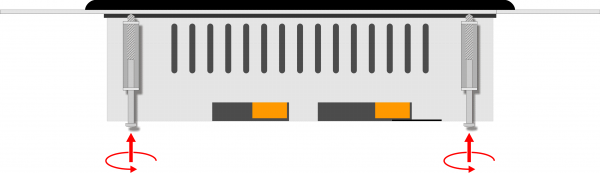
Warning: after putting the pin of fixing, do only half rotation to not tear the frame! • Please read carefully.
• See technical notes on Weidmuller terminals BLZF, BLZ and B2L.Types of Connectors
Family Wire Section
no end capsWire section
with end capsCharacteristics
of contactTools 
BLZF 3.5 0.3-1.50 mm2 0.3-1 mm2 
Open the self-locking, spring clip terminals with a flat blade screwdriver to DIN 5264-A as shown below
See the table below for recommended cap ends
To crimp the cap ends to the wire use the tool below
B2L 3.5 0.3-1.00 mm2 0,3-0.5 mm2 
BLZF 5.08 0.3-2.50 mm2 0.3-2.00 mm2 
BLZ 5.00 0.2-2.50 mm2 0.1-1 mm2 
The screw terminals can be tightened with a flat blade screwdriver to DIN 5264 as shown in fig.4.7
Tightening torque: 0.4 - 0.5 Nm.For a safer cabling, always use wire end caps
Tools
End caps
Wire section End cap section Make Model 0.1-0.3 mm2 0.95 mm2 Cembre PKE 308 0.3-0.5 mm2 1.32 mm2 Cembre PKE 508 BM BM00601 1 mm2 2.5mm2 BM00603 PK 108 BM BM00603 End cap crimping tool
 Use a crimp tool type “Cembre ND#4
cod. 2590086”
Use a crimp tool type “Cembre ND#4
cod. 2590086”
Screwdrivers
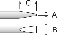 Screwdriver for opening self-locking spring clip terminals:
A = 0.6mm
B = 2.5mm max
C = 7 mm min
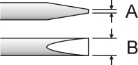 Screwdriver for tightening screw terminals:
A = 0.6mm
B = 3.5mm
Procedure

Strip 10mm of copper wire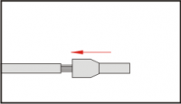
Fit the end cap and crimp it with a crimping tool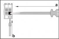
a) fit the screwdriver without turning it
b) fit the cable in the terminal
Remove the screwdriver3. Electric Characteristics and_ wiring
Slot Supply

The cabling must be carried out by specialist personnel and fitted with suitable anti-static precautions.
Before handling the controller, disconnect the power and all parts connected to it.
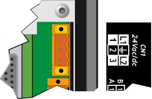
To guarantee compliance with EC regulations, the power supply must have a galvanic isolation of at least 1500Vac.Power supply 24 Vdc Voltage range 22 - 27 Vdc Max. absorption 30W CN1 Terminal Symbol Description 

1 L1/+ DC power positive 2 GROUND Gnd-PE (signals) 3 L2/- DC power 0V Connection examples for 24Vdc power supply
Use an isolated power unit with 24Vdc +/-5% output conform to EN60950-1. 
Use two separate power units: one for the control circuit and one for the power circuit 
For a single power unit, use two separate lines: one for the control and one for the power 
DO NOT use the same lines for the power circuit and the controller Slot 2
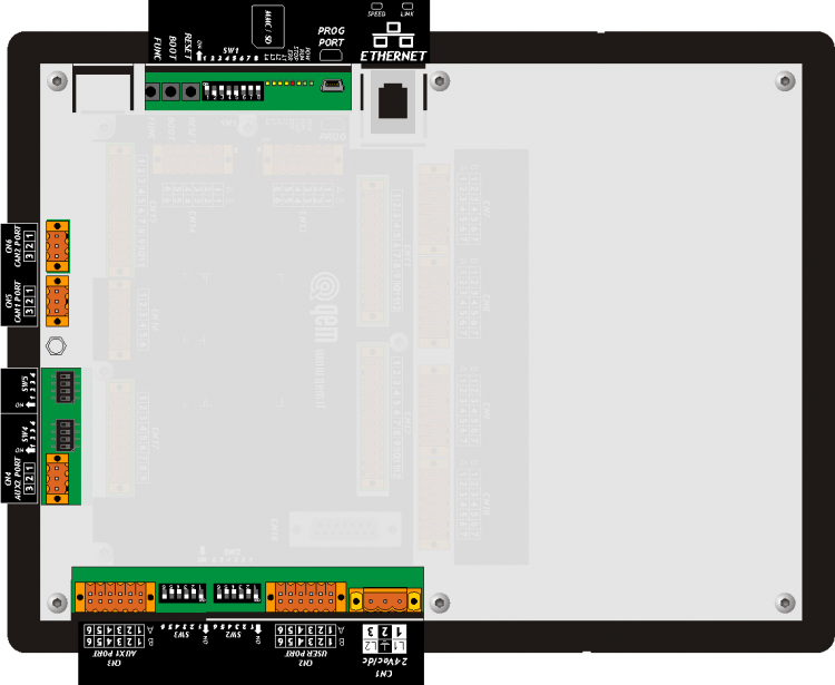
Serial Port Connections
CN2 Terminal RS232 RS422 RS485 Description 
1A - - A Terminal A - RS485 2A - - B Terminal B - RS485 3A 0V 0V 0V USER PORT common 4A 0V 0V 0V USER PORT common 5A TX - - Terminal TX - RS232 6A Terra 1B - RX - Terminal RX - RS422 2B - RXN - Terminal RX N - RS422 3B - TX - Terminal TX - RS422 4B - TXN - Terminal TX N - RS422 5B RX - - Terminal RX - RS232 6B Ground Setup of USER PORT electric standard
CN3 Terminal RS232 RS422 RS485 Description 1A - - A Terminal A - RS485 2A - - B Terminal B - RS485 3A 0V 0V 0V USER PORT common 4A 0V 0V 0V USER PORT common 5A TX - - Terminal TX - RS232 6A Ground 1B - RX - Terminal RX - RS422 2B - RXN - Terminal RX N - RS422 3B - TX - Terminal TX - RS422 4B - TXN - Terminal TX N - RS422 5B RX - - Terminal RX - RS232 6B Ground Setup of AUX1 PORT electric standard
CN4 Terminal Symbol Description 
1 0V RS485 serial common 2 B Terminal RS485 B 3 A Terminal RS485 A Setup of AUX2 PORT polarisation and termination resistances
CAN1 PORT
CAN2 PORTTerminal Symbol Description 1 0V CAN common 2 CAN L Terminal CAN L 3 CAN H Terminal CAN H Setup of CAN1 and CAN2 PORT Termination resistances
ETHERNET PORT Description 
Connector RJ45.
LED:
* LINK: green led = cable connected (led on signals the cable is connected to both ends)
* DATA: yellow led = data transmission (flashing led signals data transmission)
Memory card slot (marked by an arrow) Serial Port Characteristics
The USB mini-B connector does not support USB electrical standards, it can only be used with an interface IQ009 or IQ013. It is used for the transfer and debugging of the application program in the CPU.
Electrical standard TTL (Use serial interface IQ009 or IQ013) Communication speed Min. 9.6 Kbaud - max 115200 Kbaud
settable by dip1 and 2 of the switch SW1Insulation None .

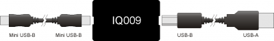

Connection between Qmove+ e PC using the accessory IQ009 .

Connection between Qmove+ and a device fitted with a RS232 serial port (e.g. a MODEM), using the interface IQ013 Communication speed 4800, 9600, 19200, 38400, 57600, 115200 baud Communication mode Full duplex Operating mode Referred to 0V Max. number of devices connected on the line 1 Max. cable length 15 m Input impedence > 3 Kohm Short-circuit current limit 7 mA 

Communication speed 4800, 9600, 19200, 38400, 57600, 115200 baud Communication mode Full duplex Operating mode Differential Max. number of devices connected on the line 1 Max. cable length 1200 m Input impedence > 12 Kohm Short-circuit current limit 35 mA 


To activate the internal termination resistance see paragraph Setup of USER PORT electric standard, Setup of AUX1 PORT electric standard or Setup of AUX2 PORT polarization and termination resistances .
Communication speed 4800 baud (only if used with SERCOM and/or MODBUS device),
9600 baud, 19200 baud, 38400 baud, 57600 baudCommunication mode Half duplex Operating mode Differential Max. number of devices connected on the line 32 Max. cable length 1200 m Input impedence > 12 Kohm Short-circuit current limit 35 mA 

To activate the internal termination resistance see paragraph Setup Termination resistances
.
Communication speed 125, 250, 500, 1000 Kbit/s Max. number of Drivers/Receivers on the line 100 Max. cable lengths 500m @ 125Kbit/s, 250m @ 250Kbit/s, 100m @ 500Kbit/s, 25m @ 1000Kbit/s Input impedence >15Kohm Short-circuit current limit 45mA 


CAN BUS connection examples.
Caution:
Close DIP's JP1 and JP2 and insert the termination resistances (RL, RH) on the last device of the chain.Ethernet Interface 10/100 Base T (IEEE 802.3) on RJ45 connector.
Connection between Qmove + and PC:


Qmove+ Cross-over cable EIA/TIA-568A/B PC Type of Memory Card to use MMC, SD and SDHC up to 8GB
For proper operation it is necessary that the device conforms to the standards set by “SD Association” (www.sdcard.org) or “Multi Media Card Association” (www.mmca.org)..
To use the Memory Cards they must first be formatted with FAT16 or FAT32 file system. Slot 3 – 1MG8F Card Connectors

Digital Inputs

The electrical features are given in paragraph Electrical Features.
The wiring examples are given in paragraph Connection examplesCN11 Terminal Symbol Description Address 
1 I01(PNP) PNP type fast input I01 External terminal configuration1) FREQ12) 2 I01(NPN) PNP type fast input I01 3 0V Common for digital inputs 4 I1 Input I1 3.INP01 5 I2 Input I2 3.INP02 6 I3 Input I3 3.INP03 7 I4 Input I4 3.INP04 8 I5 Input I5 3.INP05 9 I6 Input I6 3.INP06 10 I7 Input I7 3.INP07 11 I8 Input I8 3.INP08 12 0V Common for digital inputs
CN12 Terminal Symbol Description Address 1 I02(PNP) PNP type fast input I02 External terminal configuration1) FREQ22) 2 I02(NPN) NPN type fast input I02 3 0V Common for digital inputs 4 I9 Input I9 3.INP09 5 I10 Input I10 3.INP10 6 I11 Input I11 3.INP11 7 I12 Input I12 3.INP12 8 I13 Input I13 3.INP13 9 I14 Input I14 3.INP14 10 I15 Input I15 3.INP15 11 I16 Input I16 3.INP16 12 0V Common for digital inputs
CN13 Terminal Symbol Description Address 1 I03(PNP) PNP type fast input I03 External terminal configuration1) 1.INT09 2 I03(NPN) NPN type fast input I03 3 0V Common for digital inputs 4 I17 Input I17 3.INP17 5 I18 Input I18 3.INP18 6 I19 Input I19 3.INP19 7 I20 Input I20 3.INP20 8 I21 Input I21 3.INP21 9 I22 Input I22 3.INP22 10 I23 Input I23 3.INP23 11 I24 Input I24 3.INP24 12 0V Common for digital inputs
1) NPN type fast input configuration:
Terminal 1: connect to 12-24Vdc of the power unit
Terminal 2: input
PNP type fast input configuration:
Terminal 1: input
Terminal 2: connect to 0V (terminal 3)CN14 Terminal Symbol Description Address 1 I04(PNP) PNP type fast input I04 External terminal configuration1) 1.INT10 2 I04(NPN) NPN type fast input I04 3 0V Common for digital inputs 4 I25 Input I25 3.INP25 5 I26 Input I26 3.INP26 6 I27 Input I27 3.INP27 7 I28 Input I28 3.INP28 8 I29 Input I29 3.INP29 9 I30 Input I30 3.INP30 10 I31 Input I31 3.INP31 11 I32 Input I32 3.INP32 12 0V Common for digital inputs
1) NPN type fast input configuration:
Terminal 1: connect to 12-24Vdc of the power unit
Terminal 2: input
PNP type fast input configuration:
Terminal 1: input
Terminal 2: connect to 0V (terminal 3)The electrical features are given in paragraph Electrical features.
The wiring examples are given in paragraph Connection examplesCN15 Terminal Symbol Description Address 
1A Internal bridge 1A -1B 1) 2A PHA1 Phase A Count 1
PNP Push-Pull2)3.INP33 3.CNT01 3A PHB1 Phase B 3.INP34 4A Z1 Z 1.INT01 5A 0V Common for count inputs 6A 0V 7A 0V 1B Internal bridge 1A -1B3) 2B PHA1+ + PHA Count 1
Line Driver3.INP33 3.CNT01 3B PHB1+ + PHB 3.INP34 4B Z1+ + Z 1.INT01 5B PHA1- - PHA 6B PHB1- - PHB 7B Z1- - Z
2) PNP/Push-Pull type count input configuration:
Terminal 5B: connect to terminal 5A
Terminal 6B: connect to terminal 6A
Terminal 7B: connect to terminal 7ACN16 Terminal Symbol Description Address 1A Internal bridge 1A -1B 1) 2A PHA2 Phase A Count 2
PNP Push-Pull2)3.INP35 3.CNT02 3A PHB2 Phase B 3.INP36 4A Z2 Z 1.INT02 5A 0V Common for count inputs 6A 0V 7A 0V 1B Internal bridge 1A -1B3) 2B PHA2+ + PHA Count 2
Line Driver3.INP35 3.CNT02 3B PHB2+ + PHB 3.INP36 4B Z2+ + Z 1.INT02 5B PHA2- - PHA 6B PHB2- - PHB 7B Z2- - Z
2) PNP/Push-Pull type count input configuration:
Terminal 5B: connect to terminal 5A
Terminal 6B: connect to terminal 6A
Terminal 7B: connect to terminal 7ACN17 Terminal Symbol Description Address 1A Internal bridge 1A -1B 1) 2A PHA3 Phase A Count 3
PNP Push-Pull2)3.INP37 3.CNT03 3A PHB3 Phase B 3.INP38 4A Z3 Z 1.INT03 5A 0V Common for count inputs 6A 0V 7A 0V 1B Internal bridge 1A -1B3) 2B PHA3+ + PHA Count 3
Line Driver3.INP37 3.CNT03 3B PHB3+ + PHB 3.INP38 4B Z3+ + Z 1.INT03 5B PHA3- - PHA 6B PHB3- - PHB 7B Z3- - Z
2) PNP/Push-Pull type count input configuration:
Terminal 5B: connect to terminal 5A
Terminal 6B: connect to terminal 6A
Terminal 7B: connect to terminal 7ACN18 Terminal Symbol Description Address 1A Internal bridge 1A -1B 1) 2A PHA4 Phase A Count 4
PNP Push-Pull2)3.INP39 3.CNT04 3A PHB4 Phase B 3.INP40 4A Z4 Z 1.INT04 5A 0V Common for count inputs 6A 0V 7A 0V 1B Internal bridge 1A -1B3) 2B PHA4+ + PHA Count 4
Line Driver3.INP39 3.CNT04 3B PHB4+ + PHB 3.INP40 4B Z4+ + Z 1.INT04 5B PHA4- - PHA 6B PHB4- - PHB 7B Z4- - Z
2) PNP/Push-Pull type count input configuration:
Terminal 5B: connect to terminal 5A
Terminal 6B: connect to terminal 6A
Terminal 7B: connect to terminal 7ACN19 Terminal Symbol Description Address 1A Internal bridge 1A -1B 1) 2A PHA5 Phase A Count 5
PNP Push-Pull2)3.INP41 3.CNT05 3A PHB5 Phase B 3.INP42 4A Z5 Z 1.INT05 5A 0V Common for count inputs 6A 0V 7A 0V 1B Internal bridge 1A -1B3) 2B PHA5+ + PHA Count 5
Line Driver3.INP41 3.CNT05 3B PHB5+ + PHB 3.INP42 4B Z5+ + Z 1.INT05 5B PHA5- - PHA 6B PHB5- - PHB 7B Z5- - Z
2) PNP/Push-Pull type count input configuration:
Terminal 5B: connect to terminal 5A
Terminal 6B: connect to terminal 6A
Terminal 7B: connect to terminal 7ACN20 Terminal Symbol Description Address 1A Internal bridge 1A -1B 1) 2A PHA6 Phase A Count 6
PNP Push-Pull2)3.INP43 3.CNT06 3A PHB6 Phase B 3.INP44 4A Z6 Z 1.INT06 5A 0V Common for count inputs 6A 0V 7A 0V 1B Internal bridge 1A -1B3) 2B PHA6+ + PHA Count 6
Line Driver3.INP43 3.CNT06 3B PHB6+ + PHB 3.INP44 4B Z6+ + Z 1.INT06 5B PHA6- - PHA 6B PHB6- - PHB 7B Z6- - Z
2) PNP/Push-Pull type count input configuration:
Terminal 5B: connect to terminal 5A
Terminal 6B: connect to terminal 6A
Terminal 7B: connect to terminal 7ACN21 Terminal Symbol Description Address 1A Internal bridge 1A -1B 1) 2A PHA7 Phase A Count 7
PNP Push-Pull2)3.INP45 3.CNT07 3A PHB7 Phase B 3.INP46 4A Z7 Z 1.INT07 5A 0V Common for count inputs 6A 0V 7A 0V 1B Internal bridge 1A -1B3) 2B PHA7+ + PHA Count 7
Line Driver3.INP45 3.CNT07 3B PHB7+ + PHB 3.INP46 4B Z7+ + Z 1.INT07 5B PHA7- - PHA 6B PHB7- - PHB 7B Z7- - Z
2) PNP/Push-Pull type count input configuration:
Terminal 5B: connect to terminal 5A
Terminal 6B: connect to terminal 6A
Terminal 7B: connect to terminal 7ACN22 Terminal Symbol Description Address 1A Internal bridge 1A -1B 1) 2A PHA8 Phase A Count 8
PNP Push-Pull2)3.INP47 3.CNT08 3A PHB8 Phase B 3.INP48 4A Z8 Z 1.INT08 5A 0V Common for count inputs 6A 0V 7A 0V 1B Internal bridge 1A -1B3) 2B PHA8+ + PHA Count 8
Line Driver3.INP47 3.CNT08 3B PHB8+ + PHB 3.INP48 4B Z8+ + Z 1.INT08 5B PHA8- - PHA 6B PHB8- - PHB 7B Z8- - Z
2) PNP/Push-Pull type count input configuration:
Terminal 5B: connect to terminal 5A
Terminal 6B: connect to terminal 6A
Terminal 7B: connect to terminal 7AAnalog Inputs
The electrical features are given in paragraph Electrical features.
The wiring examples are given in paragraph Connection examplesCN28 Terminal Symbol Description Address 
1 GAI Common for analog inputs 2 IA1 analog input 1 3.AI01 3 SEL1V Analog input selector 1 voltmetric 0-10V1) 4 SEL1C Analog input selector 1 amperometric 0-20mA2) 5 GAI Common for analog inputs 6 IA2 analog input 2 3.AI02 7 SEL2V Analog input selector 2 voltmetric 0-10V3) 8 SEL2C Analog input selector 2 amperometric 0-20mA4) 9 VREF Reference voltage
CN29 Terminal Symbol Description Address 3 GAI Common for analog inputs 2 IA3 analog input 3 3.AI03 3 SEL3V Analog input selector 3 voltmetric 0-10V1) 4 SEL3C Analog input selector 3 amperometric 0-20mA2) 5 GAI Common for analog inputs 6 IA4 analog input 4 3.AI04 7 SEL4V Analog input selector 4 voltmetric 0-10V3) 8 SEL4C Analog input selector 4 amperometric 0-20mA4) 9 VREF Reference voltage Digital Outputs
The electrical features are given in paragraph Electrical features.
The connection examples are given in paragraph Connection examplesCN7 Terminal Symbol Description Address 
1 V+ Output supply in (12÷28Vdc) 2 O1 Digital output 1 3.OUT01 3 O2 Digital output 2 3.OUT02 4 V- Common for output supply 5 O3 Digital output 3 3.OUT03 6 O4 Digital output 4 3.OUT04 7 V- Common for output supply 8 O5 Digital output 5 3.OUT05 9 O6 Digital output 6 3.OUT06 10 O7 Digital output 7 3.OUT07 11 O8 Digital output 8 3.OUT08 CN8 Terminal Symbol Description Address 1 V+ Output supply in (12-28Vdc) 2 O9 Digital output 9 3.OUT09 3 O10 Digital output 10 3.OUT10 4 V- Common for output supply 5 O11 Digital output 11 3.OUT11 6 O12 Digital output 12 3.OUT12 7 V- Common for output supply 8 O13 Digital output 13 3.OUT13 9 O14 Digital output 14 3.OUT14 10 O15 Digital output 15 3.OUT15 11 O16 Digital output 16 3.OUT16 CN9 Terminal Symbol Description Address 1 V+ Output supply in (12-28Vdc) 2 O17 Digital output 17 3.OUT17 3 O18 Digital output 18 3.OUT18 4 V- Common for output supply 5 O19 Digital output 19 3.OUT19 6 O20 Digital output 20 3.OUT20 7 V- Common for output supply 8 O21 Digital output 21 3.OUT21 9 O22 Digital output 22 3.OUT22 10 O23 Digital output 23 3.OUT23 11 O24 Digital output 24 3.OUT24 CN10 Terminal Symbol Description Address 1 V+ Output supply in (12-28Vdc) 2 O25 Digital output 25 3.OUT25 3 O26 Digital output 26 3.OUT26 4 V- Common for output supply 5 O27 Digital output 27 3.OUT27 6 O28 Digital output 28 3.OUT28 7 V- Common for output supply 8 O29 Digital output 29 3.OUT29 9 O30 Digital output 30 3.OUT30 10 O31 Digital output 31 3.OUT31 11 O32 Digital output 32 3.OUT32 The electrical features are given in paragraph Electrical features.
The wiring examples are given in paragraph Connection examplesCN23 Terminal Symbol Description Address 
1A - n.c. 2A DIR1+ DIRECTION output 1 Push-Pull Line Driver 3.PULSE01 3A STEP1+ STEP output 1 4A DIR2+ DIRECTION output 2 3.PULSE02 5A STEP2+ STEP output 2 6A 0V Common for stepper outputs 1B - n.c. 2B DIR1- Complementary output DIRECTION 1 Complementary outputs for use
in drivers with Line-Driver inputs3B STEP1- Complementary output STEP 1 4B DIR2- Complementary output DIRECTION 2 5B STEP2- Complementary output STEP 2 6B 0V Common for stepper outputs CN24 Terminal Symbol Description Address 1A - n.c. 2A DIR1+ DIRECTION output 3 Push-Pull Line Driver 3.PULSE03 3A STEP1+ STEP output 3 4A DIR2+ DIRECTION output 4 3.PULSE04 5A STEP2+ STEP output 4 6A 0V Common for stepper outputs 1B - n.c. 2B DIR1- Complementary output DIRECTION 3 Complementary outputs for use
in drivers with Line-Driver inputs3B STEP1- Complementary output STEP 3 4B DIR2- Complementary output DIRECTION 4 5B STEP2- Complementary output STEP 4 6B 0V Common for stepper outputs CN25 Terminal Symbol Description Address 1A - n.c. 2A DIR5+ DIRECTION output 5 Push-Pull Line Driver 3.PULSE05 3A STEP5+ STEP output 5 4A - n.c. 5A - n.c. 6A 0V Common for stepper outputs 1B - n.c. 2B DIR5- Complementary output DIRECTION 5 Complementary outputs for use
in drivers with Line-Driver inputs3B STEP5- Complementary output STEP 5 4B - n.c. 5B - n.c. 6B 0V Common for stepper outputs Analog Outputs
The electrical features are given in paragraph Electrical features.
The wiring examples are given in paragraph Connection examplesCN26 Terminal Symbol Description Address 
1 GAO Common for analog outputs 2 AO1 Analog output 1 3.AN01 3 AO2 Analog output 2 3.AN02 4 GAO Common for analog outputs 5 AO3 Analog output 3 3.AN03 6 AO4 Analog output 4 3.AN04 CN27 Terminal Symbol Description Address 1 GAO Common for analog outputs 2 AO5 Analog output 5 3.AN05 3 AO6 Analog output 6 3.AN06 4 GAO Common for analog outputs 5 AO7 Analog output 7 3.AN07 6 AO8 Analog output 8 3.AN08 Electrical Characteristics
The electrical characteristics of the hardware are given below.
The maximum and minimum frequencies, and real acquisition times, may depend on eventual additional software filters, for example see the system variable “QMOVE:sys004” at paragraph System Variables.Type of polarisation PNP Min. acquisition time (hardware) 3ms Isolation 1000Vrms Rated operating voltage 24Vdc Voltage of logic state 0 0-2 V Voltage of logic state 1 10.5 - 26.5 V Internal voltage drop 5V Input resistance (Ri) 2700Ω Sink current 2mA ÷ 8mA1)
1) CAUTION: If the device connected to the inputs needs a higher minimum current, inputs may not work properly.
Tipo di polarizzazione NPN / PNP Frequenza massima 200KHz Tempo min. di acquisizione (hardware) 5µs Isolamento 1000Vrms Tensione di funzionamento nominale 24Vdc Tensione stato logico 0 0÷2 V Tensione stato logico 1 10,5 ÷ 26,5 V Caduta di tensione interna 1,2 V Resistenza di ingresso 2700Ω 
The values given in the table refer to input signals A, B and Z.
The max. frequency given in the table refers to A and B phase signals with a DutyCycle = 50%
With count frequencies over 50KHz the use of Line-Driver type encoders is recommended.Type of polarisation PNP/PP Max frequency 200KHz Min. acquisition time 5µs Insulation 1000Vrms Rated operating voltage 24Vdc Voltage of logic status 0 0 - 2 V Voltage of logic status 1 10.5 - 26.5 V Internal voltage drop 1.2V Input resistance 3100Ω Line-Driver
Type of polarisation Line-Driver Max. frequency 200KHz Min. acquisition time 5µs Insulation 1000Vrms Rated operating voltage (PHx+ ? PHx-) 5Vdc Voltage of logic status 0 (PHx+ ? PHx-) 0-1.5 V Voltage of logic status 1 (PHx+ ? PHx-) 2-5 V Internal voltage drop 1.2V Input restistance 150Ω 
Type of connection Potentiometric 1KΩ-20KΩ Resolution 12bit/16bit Reference voltage output 2.5Vdc Max output current from reference 10mA Input resistance 10MΩ Max. linearity error + 0,1% Vfs Max. offset error + 0,1% Vfs S.n. 71 dB Update speed 1ms Insulation 1000 Vrms 
Type of connection Voltmetric
0-10VResolution 12bit/16bit Input resistance (Rin) 20KΩ Damage value 20V Max. linearity error + 0.1% Vfs Max. offset error + 0.1% Vfs S.n. 71 dB Update speed 1ms Insulation 1000 Vrms 
Type of connection Amperometric
(0-20 mA)Resolution 12bit/16bit Input resistance 125Ω Damage value 25 mA Max. linearity error + 0,1% Vfs Max. offset error + 0,1% Vfs S.n. 71 dB Update speed 1ms Insulation 1000 Vrms 
Switchable load Dc (PNP) Max. operating voltage 28V Insulation 1000Vpp Max. internal voltage drop 600mV Max internal resistance @ON 90mΩ Max. protection current 12A Max. operating current 2A Max. current @OFF 5µA Max switching time from ON to OFF 270µs Max switching time from OFF to ON 250µs 
Type of polarisation Push-Pull / Line-Driver Max output frequency 50KHz Insulation 1000Vpp Max. operating current 20mA 
Type of connection Common mode Insulation 1000Vrms Voltage range (minimum no load) -9.8V - +9.8V Max. offset variation depending on temperature* +/- 5mV Resolution 16bit Max. current 1mA Output variation depending on load 100 µV/mA Output resistence 249Ω 
CANbus

• On the first (1) and on the last (3) device of the chain, the termination resistances must be inserted.
• The cable shoes must be connected to ground by the fastons provided on the metal body.• To activate the internal termination resistance see paragraph Setup of CAN1 and CAN2 PORT Termination resistances Digital inputs

PNP / Push Pull count inputs

Voltmetric and amperometric analog inputs

Voltmetric and potentiometric analog inputs

Protected digital outputs

Analog outputs

4. Settings, procedures and signals

SW1 Dip DIP settings Function 
1 OFF OFF ON ON Select PROG PORT transmission speed 2 OFF ON OFF ON Baud-rate
38400Baud-rate
115200Baud-rate
19200Baud-rate
576003 OFF OFF ON ON Select USER PORT transmission speed 4 OFF ON OFF ON Baud-rate
38400Baud-rate
115200Baud-rate
19200Baud-rate
576005 CANbus baud-rate selector. See paragraph CANbus baud-rate selector 6 OFF ON Select PROG PORT functioning mode PROG PORT can also be used by SERCOM and MODBUS devices PROG PORT cannot be used by SERCOM and MODBUS devices 7 CANbus baud-rate selector. See paragraph CANbus baud-rate selector 8 OFF ON Select the USER PORT as PROG PORT1) PROG PORT normal PROG PORT on USER PORT connector
1) It is possible to use the USER PORT connector as PROG PORT with RS232 electric standard, doing this the mini-USB connector of the PROG PORT is disconnected (Setting USER PORT electric standard). For this function mode also set dip 6 of SW2 to OFF.SW1 Dip DIP settings Function 1 - - 2 - - 3 - - 4 - - 5 OFF ON OFF ON Select speed of
CANbus transmission7 OFF OFF ON ON Baud-rate
125KB/SBaud-rate
250KB/SBaud-rate
500KB/SBaud-rate
1MB/S6 - - 8 - - Led
The system led's “pow, run, stop, err” are found on the front panel and on the rear of controllers with display and only on the top of controllers without display.

The user led's “L1, L2, L3 e L4” are found on the rear:

“System Led” Signals
Leggend:
 Led ON
 Led OFF
 Led Blinking
Led Colour Status Description pow Green 
Power on Only this led on, signals the CPU reset status run Green CPU in RUN status 
CPU in READY status stop Yellow With pow on, signals the STOP status of the CPU
With pow off, signals the BOOT status of the CPUerr Red With pow off, signals a hardware error. See paragraph Hardware Error codes
With pow blinking, the flash rate gives the type of error. See paragraph err led signalserr led signals
N.
flashesError Description Recommended action 1 Bus error Bus configuration different to application software. Check the correspondence between the QMOVE application (BUS section of configuration unit) and the product configurations (cards mounted in BUS). 2 CheckSum Error Negative outcome on the integrity control of retentive variables . (see Reset Error Checksum) Restore the machine data from a backup (.DAT file) or cancel the error with in system functions and enter the values manually. 3 Index Out of Bound An array index is pointing on an inexistent element Open a unit editor in Qview development environment and use the “Edit→Go to PC” command to find the program line that is cause of the error. In general the index value has a value <1 or >array dimension. 4 Program Over Range The program selection index in the DATAGROUP has attempted to access an inexistent program. With the Qview development environment open the editor of a unit and user the “Edit→Go to PC” command to highlight the program line that has caused the error. In general the value used as index is lower than 1 or over the array dimension. 5 Step Over Range The step selection index in the DATAGROUP has attempted to access an inexistent step. With the Qview development environment open the editor of a unit and user the “Edit→Go to PC” command to highlight the program line that has caused the error. In general the value used as index is lower than 1 or over the array dimension. 6 Division By Zero The denominator of a division operation of the application program has a zero value. With the Qview development environment open the editor of a unit and user the “Edit→Go to PC” command to highlight the program line that has caused the error. 7 Syntax Error The application program has an invalid instruction This error may appear because the program counter has met the QCL END instruction. 8 Watch Dog Error A CAN module does not function correctly, or a specialist card has a hardware problem With the Qview development environment open the “Monitor→Bus” panel and the righthand column called “Watchdog Bus” indicates the card that caused the problem. 9 Stack Error The applciation program has used all permitted levels of calls to subroutines With the Qview software environment open the editor of a unit and use the “Edit→Go to PC” command to highlight the program line that caused the error. Analyse the unit execution flow, the call to subroutines nestings have a limit, over which this error is generated. Hardware error codes
During the startup sequence, if a malfunction of any peripheral is detected, the system blocks and the error is signaled by the flashing led
err while the other system led's remain off.
The number of flashes indicates the type of error according to the following table :
Number of flashes Error 1 Display 2 FPGA 3 Media 4 Bootloader 5 FW 6 Bus 7 Signal not active 8 Signal not active 9 Exception Each of these signals indicates a serious error situation. The product must be sent to the QEM aftersales service.
“User Led” signal

Led Colour Description L1Yellow Programmable in the application program by the QMOVE system variable:sys003 and used by the system functions L2 L3 L4Keys

Name Description  FUNC
FUNCPress on startup of the controller to access the System functions BOOTPress on startup of the controller to set the CPU in Boot status and then access the firmware update functions RESETReset CPU. the system is restarted restoring the initial conditions (after a startup ) Operating Overview
Foreword
This chapter covers aspects and descriptions of the product functionalities that are often related to the firmware, which enable the functionalities that enable its operation as a QEM Qmove+ programmable system.
Organization of data and memories
To best understand the terms used in this chapter, it is important to know the organisation of data and memory in a QMOVE application. QMOVE applications are programs written in QCL language that, translated in binary code, are transferred onto QMOVE hardware and saved there. In the hardware, the microprocessor runs has a program called firmware that interprets the above binary code instructions and performs the operations associated to them.
A QCL application, in addition to the instructions, is also composed of variables that the QCL instructions act on.. Some of these variables are retentive, i.e. their values remain unaltered from shut-off to start up. The flow chart below illustrates the organisation of data in a QCL application transferred to the memory of any QMOVE hardware:
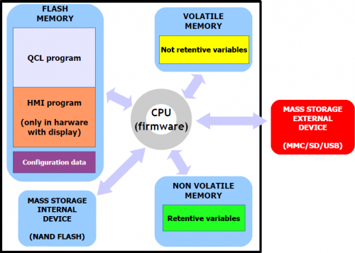
It can be noted that, the QMOVE hardware has several mass storage devices with different technology (e.g. the non volatile data memory may be a §ram tamponata rather than an eeprom or a magneto-resistiva ram, …), they have been divided in the following categories:
“Nonvolatile memory”, where the following is saved:
-
QCL Program: the series of QCL instructions translated into binary by the compiler.
-
HMI program: the series of HMI screens translated into binary by the compiler. This program only exists when the QMOVE hardware has a display.
-
Configuration data: the calibration and configuration data, e.g. the touch-screen calibration settings, the ethernet communication configuration data (IP address, etc). This data can be entered by both system functions and specigic PC software utilities.
“Non volatile data memory”, which stores:
-
Retentive variables: the group of variables that remains unaltered on a shut-off and startup (e.g. SYSTEM, ARRAYS, DATAGROUP, etc).
“Volatile data memory”, which stores:
-
Non retentive variables: the group of variables that is set to 0 at each startup (e.g. GLOBAL, ARRGBL, etc).
The volatile data memory is also used as dynamic memory. i.e. the memory used by the firmwarefor internal operations and active HMI screen management.
“Internal mass memory” is managed by a standard filesystem and is useful to save information by the DATASTORE device (read - write binary or csv files with recipes, logs, variuous setups, etc).
E' inoltre utilizzato per memorizzare il backup dell'applicativo QMOVE.“External mass storage” is managed by a standard filesystem and is useful for loading the QMOVE application, data loading/saving, firmware update or to save information by the DATASTORE device.
CPU Status
The CPU has several operating statuses. The figure below shows the main status changes from the controller startup.
The main operatiing statuses are RESET, READY, RUN and STOP.
The CPU events that determine a transition from one status to another are mainly linked to commands being sent by the development environment: Run, Reset, Stop and Restart.
Application download is the development environment procedure that allows to transfer a QMOVE application to the CPU.
Application download is the development environment procedure that allows to transfer a QMOVE application to the CPU.
The BOOT state can be used to access the firmware updating functions.
SELF-DIAGNOSIS
During the startup, after scanning the system led's, the controller performs a series of self-diagnostic operations. When any faults are detected or the operator has to be informed of any given situation, the self-doagnosis procedure is temporarily interrupted, signalling the event.
The fault signal is made by led's L1, L2 and a message is given on display (if present).System Messages
n. Led ON System Message (if display present) Description Type 1 L1System Data WRITE ERRORIndicates that a write error has occurred during the configuration data saving. B 2 L2System Data IS RESTORED FROM DEFAULTIndicates that the configuration data has been restores to the default settings. C 3 L1
L2System Data is updated
Please verify new dataIndicates that the configuration data has been converted into a new format. Check that the previous settings have been maintained. C 4 L3Firmware is updated
old: 1K31F10 1.001
new: 1K31F10 1.002Indicates that a firmware update has been made. C When the condition detected allows to continue to the start stage (type C) and waits for the FUNC button
to be pressed to continue the boot procedure.
The controller waits 5 seconds before continuing with the startup stage, without waiting for a button to be pressed.
When the situation does not allow to continue the startup stage (tipo B), the led
err flashes continuously.
SYSTEM BOOTING
During the condition SELF-DIAGNOSTICS and SYSTEM BOOTING on the instrument with the display, you see some important information about the system as shown in the following picture:
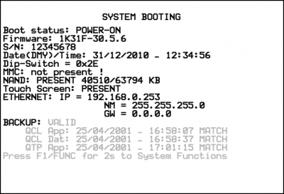
WARNING: The values shown in the diagram are examples and may change depending on the instrument in question. List of informations
Nr. Message Description 1 Boot status: POWER-ONDisplays the boot status:
POWER-ON Sterting the instrument
INIT Initializing application downloads
RESTART Restart the instrument software
BACKUP Backup operation
RESTORE Restore operation2 Firmware: 1K31F-30.5.6Displays the name, version, major release and minor release of the firmware. Example:
1K31F Firmware name
30 Version
5 Major release
6 Minor release (build)3 S/N: 12345678Serial number of the instrument. 4 Date(DMY)/Time: 31/12/2010 - 12:34:56Clock and calendar:
GG/MM/YYYY - HH:MM:SS5 Dip-Switch = 0x2EYou receive a “hexadecimal value representing the status of the switch SW1.
Is equivalent to the value of the system variable SYS002.6 MMC: PRESENT 510/31250 KBIf you inserted the MMC/SD, at this stage appear the device data as used KB (510) and total KB (31250).
In case the device does not exist message appears: “not present !”7 NAND: PRESENT 40510/63794 KBIt checks the internal device NAND and and then displays the used KB and the total KB.
In the event that the device is not found, an error is reported and appears “NAND: NOT PRESENT !”8 Touch Screen: PRESENTIn the instruments with touch screen, it is detected and then checks the calibration data.
In the event that should still be performed calibration, you receive the message “CALIBRATION REQUIRED !”.
The touch calibration is possible with the system function “Touch Calibration”.9 ETHERNET: IP = 192.168.0.253
NM = 255.255.255.0
GW = 0.0.0.0In the instruments with ethernet interface, are visualized the parameters for the address (IP), net mask (NM) and gateway (GW).
Set this parameters with the function “Set Ethernet communic. parameter”10 BACKUP: VALID
QCL App: 25/04/2001 - 16:58:07 MATCH
QCL Dat: 25/04/2001 - 16:58:37 MATCH
QTP App: 25/04/2001 - 17:01:15 MATCHChecked in NAND of a good backup and displays the creation data and time of application (QCL App), the data (QCL Dat) and the QTP data (QTP App).
If after the “BACKUP” message appears the “VALID” message means that the backup can be restored properly by using the system function “Restore from NAND”.
If after the “BACKUP” message appears the “NOT PRESENT” message means that the backup is not present.
If after the “BACKUP” message appears the “NOT VALID” message means that the backup cannot be restored properly because the checksum between the file aren't the same. After any file (QCL App, QCL Dat e QTP App), in addition to the date and time of creation, also displays additional informations:
“MATCH” indicates that the file is the same with the RUN application.
“NO MATCH” indicates that the file isn't the same with the RUN application.
“SIZE ERROR” indicates that the file size is invalid.
“NOT PRESENT” indicates that the file does not exist.11 Press F1/FUNC for 2s to System FunctionsThis message indicates that the pressure of F1 or FUNC buttons for 2 seconds, provides access to system functions as described in the procedure. The message is visible for 4 seconds. 12 !!! WARNING detected !!!
Press FUNC or F1 to continueIf during the previous stages, warning messages are displayed, wait for about 20 seconds.
If you not wait, press the F1 or FUNC keys.13 !!! ERROR detected !!!
Press FUNC or F1 to continueMessage displayed if in previous phases, you receive error messages.
To continue you are press F1 or FUNC keys.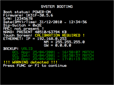
WARNING: The values shown in the diagram are examples and may change depending on the instrument in question.
For the instrument without the display, during this phase you don't see the informations.The SYSTEM FUNCTIONS status can be used to access the SYSTEM FUNCTIONS, which are special procedures that allow the user to perform various operations. For more details see the System Functions chapter.
Led status pow
 run
runStatus cause No application in memory. The condition that can put the CPU in this status RESET command. This condition can only pass onto a READY status by downloading the applicaiton, using the Qview6 development environment.
Led status pow
runStatus cause Application valid and waiting for execution. Conditions that can put the CPU in this status Application download. This condition can pass onto to the RUN or RESET statuses.
Led status pow
runStatus cause Application in execution. Condition that can put the CPU in this status RUN command. This condition can pass onto all other CPU statuses.
Led status pow
stop » runStatus cause Stop on application in execution. Condition that can put the CPU in this status A breakpoint has been encountered in the application code interpretation. This condition can pass onto all other CPU statuses.
System Functions
IMPORTANT: The use of these procedures could represent a risk (e.g. see deletion of application), therefore it is highly recommended that they are performed by qualified experts.
The system functions are spefici procedures that allow the user to perform various operations, e.g. the configuration/calibration of peripherals, data and application save/restore on/from removable mass memory, deletion of the application and management of the mass memories.
Controllers with display have some system functions that are only accessible by password and if access attempts are made the “Function is locked” message is given.All the system functions are listed below.
If the “PWD” column shows 'Y', this means that the function requires a system password (default: “123”).System Functions
n. Led ON System Function PWD Description 1 L1 01 - Reset Error Checksum - Reset error checksum.
N.B.: if the checksum error is present, the ledL1 flashes. 2 L2 02 - Copy all files MMC/SD → NAND - Copy all files from MMC/SD to NAND Flash memory. 3 L1
L2 03 - Copy all files NAND → MMC/SD - Copy all files from NAND Flash memory to MMC/SD. 4 L3 04 - Application delete Y Delete the application. 5 L1
L3 05 - Application upload from MMC/SD Y Upload the application from MMC/SD. 6 L2
L3 06 - Set Date & Time - Adjust the system clock 7 L1
L2
L3 07 - Downl. retentive data to MMC/SD - Save the retentive data on MMC/SD. 8 L4 08 - Set NEW Password Y Set a new password to access the “locked” system functions 9 L1
L4 09 - Remove all files from NAND Flash Y Cancel all files stored on the NAND Flash memory. 10 L2
L4 10 - Show NAND Flash files - List the files stored on the NAND Flash memory 11 L1
L2
L4 11 - Touch Calibration - Run the calibration procedure of the Touch Screen, if present. 12 L3
L4 12 - Set Ethernet communic. parameter - Run the setup procedure for the Ethernet communication parameters (IP address,…, etc.) 13 L1
L3
L4 13 - Backup to NAND - Run the backup of the QCL application, data and HMI application on NAND memory. 14 L2
L3
L4 14 - Restore from NAND Y Run the restore of the QCL application, data and HMI application from NAND memory. NB: To exit system functions press the keep the F1 key or FUNC button for at least two seconds.
To access the System Functions, start up the controller with FUNC button pressed.
FUNC
The QMOVE application, if present, it not executed and the led
 L1 lights up.
Use the FUNC button
to scroll through the functions.
The selected function is indicated by the combination of L1-L2-L3-L4 leds lighted up.The “System Functions” table gives the list of system functions and related led combinations.
Press the BOOT button for 2 seconds to execute the selected function.
BOOT
The POW led starts flashing to indicate taht the selected function is being executed.
POW
When the function ends the POW led stops flashing.
POW
Press the FUNC button to restart the controller.
FUNC
If the function does not complete properly the POW stops and the ERR starts flashing POW
ERRThe number of flashes indicates the type of error as shown in the table System Function Error Messages.
When a system function ends with an error, the number of led flashes
err indicates the type of error.
If there is a display, a message is given to describe the cause of the error.System Function Error Messages
Error/Number of ERR led flashes Message 1 Generic error2 Open/Exist/Create file error3 Read file error4 Write file error5 Out of Memory error6 QMos Version error7 Checksum Error8 Symbols checksum No Match9 Configuration / Symbols error10 File format error11 Format error12 Device not present or unformatted13 Application not present error14 Touch calibration failure15 File compression type not support16 Target don't match project !17 Fw version don't match project !18 File copy error19 File size error20 Crypt operation error21 Invalid Product Serial Number22 Function is locked23 Function not enabledDescription
The system runs an integrity control of retentive variables by the applicaiton of a CRC to the nonvolatile data memory. This detects any corruption and prevents the application from starting up, signalling the situation by flashing the led
err as shown in Err led signals.
For the application to function again, a new download of the application must be performed with the development environment, or the “Reset Error Checksum” system function. These operations delete the error status and zero-setsall retentive variables.The procedure:
-
Check the error status and end the funciton if no error is present.
In microQMove products, the presence of the QCL application is also checked. -
Vengono azzerati i dati ritentivi e viene visualizzato il messaggio
“Clear power down data…”fino al termine della procedura. -
Resets the retentive data and the message
“Clear power down data…”until the end of the procedure. -
End of operation
This procedure copies all files in the root and “DS” directory of the external MMC/SD or USB card to the NAND internal mass storage.
The following table gives the sequence of operations and any possible errors:
Message Description Possible errors Check DEVICE presenceChecking for the presence of the external mass storage card
On DEVICE appears MMC or USB, depending on what is selectedDevice not present or unformattedMounting device…Mounting the external mass storage card Device not present or unformattedSearching files…Searching for compatible files No Files FoundCopy <filename>….Making a copy of the files indicating the name currently in copy This procedure copies all files contained in the root and “DS” directory of the NAND internal mass storage to the external MMC/SD or USB card memory.
The following table gives the sequence of operations and any possible errors:
Message Description Possible errors Check DEVICE presenceChecking for the presence of the external mass storage card
On DEVICE appears MMC or USB, depending on what is selectedDevice not present or unformattedMounting device…Mounting external mass storage device Device not present or unformattedSearching files…Searching for compatible files No Files FoundCopy <filename>….Copying the files indicating the name of the one currently in copy This deletes the application and empties the nonvolatible data memory, deleting the QCL program and, if present, deleting the HMI program.
The following table gives the sequence of operations performed and any possible errors:
Message Description Possible errors Reset retentive dataEmpty nonvolatible data memory Write file errorDelete QCL applicationDeletion of the QCL program Write file errorDelete HMI applicationDelection of the HMI program (if display installed) Write file error
This loads an application from the external MMC/SD or USB mass memory card to the non volatile memory.
This allows to load all or one of the QCL program, HMI program and retentive data.
The external MMC/SD or USB mass memory card must contain at least one of the following files:
-
applic.bin for the compiled QCL program generated by the Qview development environment
-
applic.dat for the data file generated by the “Save Data…” procedure of the Qview development environment or by the Downl system function. for retentive data to DEVICE;
-
appqtp.bin for the compiled HMI program generated by the Qpaint development environment; it is generated by the special function “Download the project to File…”.
Message Description Possible errors Check DEVICE presenceChecking for the presence of the external mass storage card
On DEVICE appears MMC or USB, depending on what is selectedDevice not present or unformattedMounting device…Mounting external mass storage card Device not present or unformattedIf the applic.bin is present:
Message Description Possible errors Upload QCL applicationUploading the QCL program Open/Exist/Create file error
Write file error
Read file error
Out of Memory Error
QMos Version Error
Checksum Error
Symbols checksum No Match
Configuration / Symbols ErrorIf the applic.bin file is not present, an application must already be loaded in the nonvolatile memory otherwise the “Application not present” message is given.
If the applic.dat file is present:
Message Description Possible errors Upload retentive dataUploading retentive data to the nonvolatile data memory Open/Exist/Create file error
Write file error
Read file error
Out of Memory Error
QMos Version Error
Checksum Error
Symbols checksum No Match
Configuration / Symbols Error
QTP File format errorThe procedure performs the following steps:
-
Check the presence of the MMC/SD or USB card.
The“Check DEVICE presence”message is given.
On DEVICE appears MMC or USB, depending on what is selected. -
Mounting MMC/SD or USB card.\\The “Mounting device…” message is given.
-
Uploading the QCL program (applic.bin), if contained in the removable mass storage device
The“Upload QCL application”message is given. -
Uploading retentive data of the QCL program (applic.dat), if contained in the removable mass storage device
The“Upload retentive data”message is given.
NOTE: if the applic.dat file is not found, the data in the system is maintained so long as the Symbol and Configuration checksums have not been varied. If they are varied all data will be set to zero. -
Uploading the HMI program (appqtp.bin), if contained in the removable mass storage device
The“Upload HMI application”message is given. -
The file is closed and the operation ends.
This procedure sets the system clock/calendar.
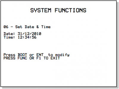
Press ENTER or the BOOT button to enter a new setting in the boxes. Each time a setting is confirmed the next box is accessed for modification. At the last box the new settings are saved.
This function creates a file on external mass storage (MMD/SD or USB) containing the retentive data values.
The file created is named “applic.dat” and is the same as the file obtained by the “Save Data…” procedure in the QView development environment. The function can only be performed if there is a valid QCL application in the controller.The procedure performs the following steps:
-
Check the presence of the MMC/SD or USB card.
The“Check DEVICE presence”message is given.
On DEVICE appears MMC or USB, depending on what is selected. -
Mounting the MMC/SD or USB card.
The“Mounting device…”message is given. -
Check the presence of the QCL program
The“Checking application presence…”message is given. -
Check the validity of the retentive data
The“Checking retentive data…”message is given. -
Open the applic.dat destination file on the external MMC/SD or USB card
The“Open destination file…”message is given. -
Write the headers in the destination file
The“Write headers to destination file”message is given. -
Write the retentive data in the destination file
The“Write data to destination file”.
NOTE: the percentage progress of the operation is given during this step -
Close the file and end the operation
This modifies the password to access the system functions. The password is a number of max 3 digits. The default password is: 123 The procedura first asks for the current password (Actual Pwd) and, if correct, then allows a new password to be entered (New Pwd).
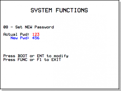
When the new password has been entered the
“saving data…”message is given to indicate that the new data is being saved.NB: if 0 (zero) is entered as a new password, the password request is disabled.
Delete all files contained on the internal NAND flash mass storage.
Unlike the “Format NAND Flash” function, this acts at a filesystem level aqnd can therefore be performed as many times as necessary.The procedure performs the following steps:
-
Calculation of the number of files contained in the internal mass storage.
-
The
“Searching files…”message is given. -
If zero files are found, the
“No Files Found”message is given and the function ends, otherwise the“Delete <filename>”is given indicating the delection of every file found. -
Close the internal storage and end procedure
This views the name and size of all files found in the internal NAND flash mass storage.
The procedure performs the following steps:
-
Calculate the number of files in the internal mass storage.
-
The
“Searching files…”message is given. -
If zero files are found the
“No Files Found”message is given and the procedure ends. -
The file name and size in bytes
“<filename> - <size>B”of each file found is shown. -
Press the BOOT key or the ENTER button again to continue and the next file when the
“Press BOOT or ENT to show next filename”message is given -
Close the internal storage device and end procedure

This views and modifies the communication parameters of the ETHERNET port.
When the function is accessed all data saved on the controller is shown.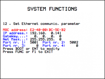
To change a parameter press ENTER and introduce the new setting.
Press ENTER to go to and change the next box.
When the last box is confirmed, the data is saved and the“saving data…”message is given
The backup procedure creates a copy of the QCL and HMI applications in execution and a dump of the retentive data, as files saved in the NAND mass storage. The files created have the following names:
-
applic.qcy identifies the file containing the QCL application (CPU)
-
appdat.qcy identifies the file containing the retentive data of the QCL application
-
appqtp.qcy identifies the file containing the HMI application
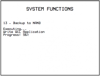
The procedure performs the following steps:
-
Check the presence of the QCL application
The“Checking application presence…”message is given. -
Create and write in NAND the QCL application backup file: applic.qcy
The“Write QCL application”message is given with the percentage progress of the operation. -
Check the presence and validity of retentive data of the QCL application
The“Checking retentive data…”message is given. -
Create and write in NAND the retentive data backup file of the QCL application: appdat.qcy
The“Write QCL data”message is given with the percentage progress of the operation. -
If the controller has a display, a check is made for the presence of the HMI application:
If the HMI application is correct the backup file appqtp.qcy is created in NAND and the“Write QTP application”message is given with the percentage progress of the operation.
If the application contains errors, the“QTP application error”message is given.
If the HMI application is not found, the“HMI application not present”message is given. -
Procedure end and system reboot.
The restore procedure allows to recover from the NAND mass storage, the saved backup files of the QCL and HMI applications and an dump of the retentive data.
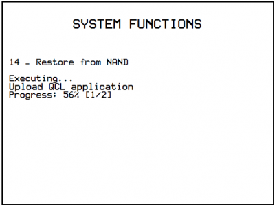
The procedure :
-
The message “Restore NAND backup” is given.
-
The NAND backup file of the QCL Application is read: applic.qcy
The message “Upload QCL application” is given, the percentage progress of the operation and the procedure step number. -
The NAND backup file of the QCL Application retentive data is read : appdat.qcy
The message “Upload retentive data” is given, the percentage progress of the operation. -
If the controller has a display, the presence of the HMI application is checked and read from the NAND back up file: appqtp.qcy.
The message “Upload HMI application” is given, the percentage progress of the operation and the procedure step number -
Procedure end and system reboot.
The use of system functions Backup to NAND and Restore from NAND allows to save in backup and restore a QMOVE application.
The backup and restore operations use the NAND internal memory device. The backup procedure creates a file copy of the QCL program, the HMI program (if the controller has a Qem display) and an image of the ritentive data.
The files created:
-
applic.qcy containing the QCL program (QCL App)
-
appdat.qcy containing the ritentive data image (QCL Dat)
-
appqtp.qcy containing the HMI program (QTP App)
The files are encrypted and only the controller that generated them can run the Restore procedure so as to safeguard unauthorised data copies. The backup file copied to external memory such as MMC/SD or USB card can be carried out with the system function Copy all NAND files -> DEVICE. A directory named “QBK” is created in the MMC/SD or USB that contains the above files. In the same way backup files can be transferred to the controller using the system function Copy all files DEVICE -> NAND. In this case, the files in the MMC/SD or USB must always be contained in the directory “QBK”.
Backup/restore is an important function that can be used in the following cases:
-
to restore the QMOVE application to a known situation (the situation at the time of the backup), if data has been changed by an operator or if the machine data has been altered for any reason.
-
when testing a new application, a backup can be made of the original, stable version. If the new application being tested is not satisfactory, the restore command will recover the original version.
Information on programming
This chapter outlines all product information that is necessary for programming, in other words during the development of a QCL application.
Development Environments
The product programming requires the Qview-5 environments to program the QCL code and if the product has a graphic display, also the Q paint-5 environment to design the screen graphics. Noth these softwares are available in the Qworkbench software package that can be downloaded as freeware from the Qem website.
The contoller has 3 slots, as indicated in chapter Back terminal blocks. The slots 4 to 12 can be declared and must be used to address recources installed in the Canopen modules.
A typical BUS declaration to use in the BUS section of the configuration unit:
  BUS
  1	1P51F	10
  2	.	.
  3	1MG8F	.
  4     C401A   .
The firmware version must naturally correspond and the specialist card name at slot 3 must be correct. This name can be obtained from the far raight column of the table: Hardware Versions.
To program with the QPaint-5 development environment it is important to select the correct target. To do so, in the environment select Project ? Target Configuration then select the right controller according to the ordering code.
This paragraph looks at how to measure an estimate of use of the product's memories. The nonvolatile memory is available to memorise the QCL program and has a capacity of 512KB.
The memory space occupied is equal to the size of the .BIN file generated by Qview. The percentage memory occupied can be viewed in the CPU panel of Qview under “Used CODE memory”, or this information can be obtained from the value of parameter “sizeapp” of the QMOS device.The nonvolatile memory available to memorise the HMI program has a capacity of 5.5MB.
The memory space occupied is equal to the size of the .BIN file generated by Qpaint, whose value (in bytes) is viewed in parameter “memqtp” of the MMIQ2 device.The nonvolatile data memory used to memorise retentive variables, has a capacity of 819KB.
The percentage memory occupied can be viewed in the CPU panel of Qview, under “Used RETENTIVE”, or this information can be obtained from the value of parameter “sizeret” of the QMOS device.The volatile data memory used to memorise non ritentive variables has a capacity that depends on various factors (e.g. the HMI and QCL program sizes, the HMI screen being viewed, etc)
The general memory of the free system, available as volatile data memory, is indicated by parameter “memfree” in the MMIQ2 device.
The PROG and USER serial ports implement the QEM proprietary communication protocol called BIN1.
The SERCOM and MODBUS devices can be used with all communication serial ports including PROG PORT. Use the following number settings during the device declaration to select the communication channel:
<QCL code>
0		PROG PORT
1		USER PORT
2		AUX1 PORT
3		AUX2 PORT
</code>
When the SERCOM and MODBUS devices use the PROG PORT or USER PORT, they address the channel only if the communication status of the device is open (st_opencom = 1). When the channel of the device is closed (st_opencom = 0) in the serial, the BIN1 protocol returns active. To force the BIN1 protocol on the PROG port (thereby preventing the SERCOM device from occupying the channel) active the SW1 dip 6.
When using the MODBUS RTU protocol with RS485 electric configuration, remember that take when the serial port is transmitting, the controller maintains the the channel (DE) active for a longer time than the “MODBUS RTU” specification. For Per questo bisogna consider a minimum time of 5 milliseconds after which it is possible to receive a new message. Anche il device SERCOM device quando, it ends a transmission, has the same time the channel is active (DE).
The Ethernet communication port uses the TCP/IP transport protocol, where the BIN1 protocol packages travel inside TCP/IP data packages. Two connections are active, identified by two communication ports freely set in the communication parameters of the Ethernet port.
In detail:
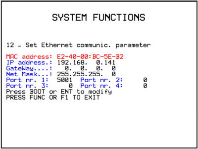 The port set in “Port nr.1:” represents a communication channel equivalent to PROG PORT.
The port set in “Port nr.2:” represents a channel equivalente to USER PORT.
The ports 3 e 4 are not used.
The port set in “Port nr.1:” represents a communication channel equivalent to PROG PORT.
The port set in “Port nr.2:” represents a channel equivalente to USER PORT.
The ports 3 e 4 are not used.
A detailed list of limitations in the QCL language:
Description Notes FSTEP,FPROG This instruction cannot be used. So there is not a direct compatibility with applications written for level A CPU's. Conversion of the application is very simple. Details of other limitations:
Description Notes Watchpoint Not available
When downloading the Qmove application, the QView-6 development environment can give error messages that are not described in the development environment manual. These errors are special and the description string given by QView-6 is generated directly by the firmware.
The table below describes possible error messages generated by the firmware.
Firmware error messages
Possible error message Description Error: SYSTEM + ARRSYS + DATAGROUP + INTDEVICE size overflow by 234bytes.Given when the retentive variables exceed the maximum limit. Error: serial port not avaliable in SERCOM or MODBUS device declaration.Given when the wrong number is used during the device declaration to select the communication channel. Error: CANOPEN device required if you use more than 3 slots.In the BUS definition more than 3 slots are being used and so the application requests the use of Canopen modules. To manage this, a CANOPEN device must be declared. Error: incorrect bus fault mode in CANOPEN declaration.The CANOPEN device declaration indicates a fault mode (last value in the declaration) that is not supported. Error: incorrect canbus speed in CANOPEN declaration.The CANOPEN device declaration indicates an invalid speed. Error: too much CANOPEN device declaration.Only one CANOPEN device can be declared. Error: absol. encoder resource num in ABSCNT device declar. is not avail.The ABSCNT device declaration indicates an inexistent resource. Error: COUNT in ABSCNT device declaration is not a simulated counter.The counter address used in the ABSCNT device declaration cannot be a simulated type (e.g. 1.CNT01). QMos version error. Unsupported instructions set.One or more statements in the project QCL are not supported by the firmware. Error: compression file type not support.The compression of the compiled QCL program is not supported by the firmware. Error: too mutch slots in bus declarations.They were declared under BUS more slots than those allowed by the hardware.
The development environment provides a series of ready-made variables that can be used by putting the word “QMOVE.” before the name. For example “QMOVE.is_suspend”, “QMOVE.sys001”, etc. This paragraph is designed to illustrate the 16 system variables called sys001-sys016, whose meaning depends on the firmware that is being used.
sys001
This is a read only variable that indicates the status of the FUNC (bit 0) and BOOT (bit 1) buttons. The following settings are possible:
0 = no button pressed.
1 = FUNC button pressed.
2 = BOOT button pressed.
3 = FUNC and BOOT buttons pressed.sys002
This variabile allows to read a dump of the SW1 dip-switches. The dump is acquired only after the controller is powered. The Bit 0 corresponds to dip 1 and so on.
NOTE: Some dips are not connected to the microprocessor and is therefore always read at logic level 0.
sys003
This variable allows the command of led's L1-L2-L3-L4. The bit 0 corresponds to L1, the bit1 to L2 and so on.
sys004
This variable allows toxet the anti-glitch filter on the phase signals in the two-way counters. The setting is expressed in KHz and refers to the signal frequency of one phase. The setting range is 30-220. The default setting is 220KHz. The variable can also be reread. The filter can be modified at any time.
sys005-16
Not used.
The term device identifies a category of software devices designed to perform more or less complex support and control actions, to solve problems tied to the automation of systems. There are two types of device: internal and external. Internal devices have their codes residing and performed by the firmware of the actual product. External devices have the code residing and executed in the “intelligent” specialist cards that have their own calculation capability. The controller can only manage internal type devices . The list of devices implemented in the firmware depends on the firmware version. This paragraph is designed to illustrate the list and characteristics of the devices available.
Firmware version 10 implements the following devices:
Device name Sampling time
minimum (msec)Sampling time
maximum (msec)Execution time (%) CANOPEN 1 250 100 CALENDAR - - 0 DATASTORE 1 20 90,5 FREQ 1 250 4,75 DAC - - 0 ANINP 1 250 14,25 COUNTER3 1 250 5,94 SERCOM 1 250 9,26 MODBUS 1 250 32,07 MMIQ2 1 10 90,5 RECDATA 1 250 5,34 QMOS - - 0 Firmware version 20 implements the following extra devices:
Device name Sampling time
minimum (msec)Sampling time
maximum (msec)Execution time (%) EANPOS 1 250 55,94 OOPOS3 1 250 27,91 HEAD2 1 125 23,75 Firmware version 30 also implements the following devices:
Device name Sampling time
minimum (msec)Sampling time
maximum (msec)Execution time (%) CAMMING3 1 250 55,94 JOINT1) 1 250 95,01
1) the effective sampling time is double the actual settingDetails of devices
CANOPEN
If the device declaration CANOPEN indicates the zero speed, then it can be set by SW1 dip's 5 and 7. The first slot to address resources that reside in Canopen modules is 4.
DATASTORE
The files processed by the device DATASTORE are all contained in the /DS directoty. If this directory does not exist, it is created automatically. The device DATASTORE can operate both with the MMC/SD card and with the internal NAND memory (not removable). To define which mass memory to operate the priority paramenter is used (0=MMC/SD, 1=NAND). If the application has to access the two supported devices frequently and the physical removal of the MMC/SD card is not required, a special setup can be used for the priority parameter that avoids having to continuously run the memory MOUNT UMOUNT. In pratice, when wanting to change memory, before running the UMOUNT command, set “priority = -1”. This avoids the UMOUNT phase is avoided in the device, making the next MOUNT command to the memory very fast.
An example of QCL code to change device:
  SUB SETMMC
    WAIT NOT Mmc:st_busy
    IF Mmc:st_mount
      Mmc:priority = -1
      UMOUNT Mmc
      WAIT NOT Mmc:st_mount
      CALL CHECK_ERR_WRN
    ENDIF
    Mmc:priority = 0
    MOUNT Mmc
    WAIT Mmc:st_mount
  ENDSUB

  SUB SETNAND
    WAIT NOT Mmc:st_busy
    IF Mmc:st_mount
      Mmc:priority = -1
      UMOUNT Mmc
      WAIT NOT Mmc:st_mount
      CALL CHECK_ERR_WRN
    ENDIF
    Mmc:priority = 1
    MOUNT Mmc
    WAIT Mmc:st_mount
    CALL CHECK_ERR_WRN
  ENDSUB
There is a particular setting of the parameters that allows to check the existence of a file in the device. Use the “filenum” parameter set to -1 and with the OPENFILE command the device, instead of opening the file, it searches for the first file in the “/DS/” directory of the selected memory. When it is found, the file name is set by the device in the parameter “filenum” (and its type in the parameter “filetype”). Setting -1 in “filenum” again and running the OPENFILE command, the next file name is found and so on. Every time an OPENFILE operation is run with filenum different to -1, the search loog is closed. When the search has ended and there are no more files present, then the device will set as answer to the command OPENFILE “filenum = -2”. The execution of the command is signalled by the flag st_busy = 0. If the file extension is not HEX or CSV, the file is ignored by the search. If the file name is not compatible with those managed by DATASTORE (numbers 0 to 9999999) then “filenum” will remain set to -1 and a warning is given.
RECDATA
The device can memorise up to 10000 step.
QMOS
The parameter “frwuvalue01” contains the number value of the product serial number.
FREQ
To define the input associated to the device FREQ use the number field provided in the device declaration. The availability of frequency inputs has to be checked with the hardware version of the product. To ricavare the relation between number and terminal pin, use the information contained in the “Address” column given in the terminal tables.
CAMMING3
The parameters related to the sectors (CodeQm, CodeQs…) are not retentive. On startup they always take on the value 0.
5. Accessories available
-
-