This is an old revision of the document!
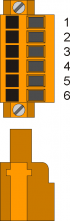
Specialization card 1MG3F rel.02

Informations
| |
||||
| Document: | MIM1MG3F02 | |||
|---|---|---|---|---|
| Description: | Installation and maintenance manual | |||
| Editor: | Riccardo Furlato | |||
| Approver | Gabriele Bazzi | |||
| Link: | http://www.qem.eu/doku/doku.php/strumenti/qmoveplus/mim1mg3f02 | |||
| Language: | English | |||
| Document Release | Hardware Release | Description | Note | Date |
| 01 | 01 | New manual | 27/11/2014 | |
| 02 | 02 | New card | See the document http://www.qem.eu/doku/doku.php/strumenti/qmoveplus/1mg3f01_1mg3f02 , to check the differences between the two hardware releases | 11/03/2015 |
1. Description
The 1MG3F is a specialization card for Qmove+ series.
1.1 Equipment
 | 16 standard digital inputs (+8 alternative inputs to 4 counters) |
 | 2 rapid digital inputs |
 | 4 bidirectional counters |
 | 2 analog inputs |
 | 8 digital outputs |
 | 4 analog outputs |
 | 4 step-direction outputs |
2. Connections
2.1 Digital inputs
2.1.1 16 standard digital inputs + 2 rapid inputs
 | The electriccal features are given in paragraph Electrical features. The wiring examples are given in paragraph Connection examples |
|---|
| CN11 | Terminal | Symbol | Description | Address | |
|---|---|---|---|---|---|
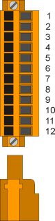 | 1 | I01(PNP) | PNP type rapid input I01 | Externally configurable terminals1) | 1.INT05 FREQ12) |
| 2 | I01(NPN) | Rapid input I01 type NPN | |||
| 3 | 0V | Common digital inputs | |||
| 4 | I1 | Input I1 | 3.INP01 | ||
| 5 | I2 | Input I2 | 3.INP02 | ||
| 6 | I3 | Input I3 | 3.INP03 | ||
| 7 | I4 | Input I4 | 3.INP04 | ||
| 8 | I5 | Input I5 | 3.INP05 | ||
| 9 | I6 | Input I6 | 3.INP06 | ||
| 10 | I7 | Input I7 | 3.INP07 | ||
| 11 | I8 | Input I8 | 3.INP08 | ||
| 12 | 0V | Common for digital inputs | |||
| CN12 | Terminal | Symbol | Description | Address | |
|---|---|---|---|---|---|
| | 1 | I02(PNP) | PNP type rapid input I02 | Externally configurable terminals1) | 1.INT06 FREQ22) |
| 2 | I02(NPN) | NPN type rapid input I02 | |||
| 3 | 0V | Common for digital inputs | |||
| 4 | I9 | Input I9 | 3.INP09 | ||
| 5 | I10 | Input I10 | 3.INP10 | ||
| 6 | I11 | Input I11 | 3.INP11 | ||
| 7 | I12 | Input I12 | 3.INP12 | ||
| 8 | I13 | Input I13 | 3.INP13 | ||
| 9 | I14 | Input I14 | 3.INP14 | ||
| 10 | I15 | Input I15 | 3.INP15 | ||
| 11 | I16 | Input I16 | 3.INP16 | ||
| 12 | 0V | Common for digital inputs | |||
2.1.2 4 bidirectional counter inputs 200KHz
| The electrical features are given in paragraph Electrical features. The wiring examples are given in paragraph Connection examples |
|---|
| CN7 | Terminal | Symbol | Description | Address | ||
|---|---|---|---|---|---|---|
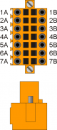 | 1A | Internal bridge 1A -1B | ||||
| 2A | PHA1 | Phase A count 1 | PNP Push-Pull1) | 3.INP17 | 3.CNT01 | |
| 3A | PHB1 Phase B count 1 | 3.INP18 | ||||
| 4A | Z1 | Z count 1 | 1.INT01 | |||
| 5A | 0V | Common for count inputs | ||||
| 6A | 0V | |||||
| 7A | 0V | |||||
| 1B | Internal bridge 1A -1B | |||||
| 2B | PHA1+ | + PHA count 1 | Line Driver | 3.INP17 | 3.CNT01 | |
| 3B | PHB1+ | + PHB count 1 | 3.INP18 | |||
| 4B | Z1+ | + Z count 1 | 1.INT01 | |||
| 5B | PHA1- | - PHA count 1 | ||||
| 6B | PHB1- | - PHB count 1 | ||||
| 7B | Z1- | - Z count 1 | ||||
1)
PNP/Push-Pull type count configuration:
Terminal 5B: connect to terminal 5A
Terminal 6B: connect to terminal 6A
Terminal 7B: connect to terminal 7A
Terminal 5B: connect to terminal 5A
Terminal 6B: connect to terminal 6A
Terminal 7B: connect to terminal 7A
| CN8 | Terminal | Symbol | Description | Address | ||
|---|---|---|---|---|---|---|
| | 1A | Internal bridge 1A -1B | ||||
| 2A | PHA2 | Phase A count 2 | PNP Push-Pull1) | 3.INP19 | 3.CNT02 | |
| 3A | PHB2 | Phase B count 2 | 3.INP20 | |||
| 4A | Z2 | Z count 2 | 1.INT02 | |||
| 5A | 0V | Common for count inputs | ||||
| 6A | 0V | |||||
| 7A | 0V | |||||
| 1B | Internal bridge 1A -1B | |||||
| 2B | PHA2+ | + PHA count 2 | Line Driver | 3.INP19 | 3.CNT02 | |
| 3B | PHB2+ | + PHB count 2 | 3.INP20 | |||
| 4B | Z2+ | + Z count 2 | 1.INT02 | |||
| 5B | PHA2- | - PHA count 2 | ||||
| 6B | PHB2- | - PHB count 2 | ||||
| 7B | Z2- | - Z count 2 | ||||
1)
PNP/Push-Pull type count configuration:
Terminal 5B: connect to terminal 5A
Terminal 6B: connect to terminal 6A
Terminal 7B: connect to terminal 7A
Terminal 5B: connect to terminal 5A
Terminal 6B: connect to terminal 6A
Terminal 7B: connect to terminal 7A
| CN9 | Terminal | Symbol | Description | Address | ||
|---|---|---|---|---|---|---|
| | 1A | Internal bridge 1A -1B | ||||
| 2A | PHA3 | Phase A count 3 | PNP Push-Pull1) | 3.INP21 | 3.CNT03 | |
| 3A | PHB3 | Phase B count 3 | 3.INP22 | |||
| 4A | Z3 | Z count 3 | 1.INT03 | |||
| 5A | 0V | Common for count inputs | ||||
| 6A | 0V | |||||
| 7A | 0V | |||||
| 1B | Internal bridge 1A -1B | |||||
| 2B | PHA3+ | + PHA count 3 | Line Driver | 3.INP21 | 3.CNT03 | |
| 3B | PHB3+ | + PHB count 3 | 3.INP22 | |||
| 4B | Z3+ | + Z count 3 | 1.INT03 | |||
| 5B | PHA3- | - PHA count 3 | ||||
| 6B | PHB3- | - PHB count 3 | ||||
| 7B | Z3- | - Z count 3 | ||||
1)
PNP/Push-Pull type count configuration:
Terminal 5B: connect to terminal 5A
Terminal 6B: connect to terminal 6A
Terminal 7B: connect to terminal 7A
Terminal 5B: connect to terminal 5A
Terminal 6B: connect to terminal 6A
Terminal 7B: connect to terminal 7A
| CN10 | Terminal | Symbol | Description | Address | ||
|---|---|---|---|---|---|---|
| | 1A | Internal bridge 1A -1B | ||||
| 2A | PHA4 | Phase A count 4 | PNP Push-Pull1) | 3.INP23 | 3.CNT04 | |
| 3A | PHB4 | Phase B count 4 | 3.INP24 | |||
| 4A | Z4 | Z count 4 | 1.INT04 | |||
| 5A | 0V | Common for count inputs | ||||
| 6A | 0V | |||||
| 7A | 0V | |||||
| 1B | Internal bridge 1A -1B | |||||
| 2B | PHA4+ | + PHA count 4 | Line Driver | 3.INP23 | 3.CNT04 | |
| 3B | PHB4+ | + PHB count 4 | 3.INP24 | |||
| 4B | Z4+ | + Z count 4 | 1.INT04 | |||
| 5B | PHA4- | - PHA count 4 | ||||
| 6B | PHB4- | - PHB count 4 | ||||
| 7B | Z4- | - Z count 4 | ||||
1)
PNP/Push-Pull type count configuration:
Terminal 5B: connect to terminal 5A
Terminal 6B: connect to terminal 6A
Terminal 7B: connect to terminal 7A
Terminal 5B: connect to terminal 5A
Terminal 6B: connect to terminal 6A
Terminal 7B: connect to terminal 7A
2.2 Analog inputs
2.2.1 4 potentiometric, voltmetric and amperometric analog inputs 12bit
| The electrical features are given in section Electrical features. The connection examples are provided in section Electrical features |
|---|
| CN7 | Terminal | Simbol | Description | Address |
|---|---|---|---|---|
 | 1 | V1+ | Outputs power input O1÷O8 (12÷28V dc) | |
| 2 | O1 | Digital output 1 | 3.OUT01 | |
| 3 | O2 | Digital output 2 | 3.OUT02 | |
| 4 | V1- | Outputs power input O1÷O8 (0V dc) | ||
| 5 | O3 | Digital output 3 | 3.OUT03 | |
| 6 | O4 | Digital output 4 | 3.OUT04 | |
| 7 | V1- | Outputs power input O1÷O8 (0V dc) | ||
| 8 | O5 | Digital output 5 | 3.OUT05 | |
| 9 | O6 | Digital output 6 | 3.OUT06 | |
| 10 | O7 | Digital output 7 | 3.OUT07 | |
| 11 | O8 | Digital output 8 | 3.OUT08 |
| CN8 | Terminal | Simbol | Description | Address |
|---|---|---|---|---|
| | 1 | V2+ | Outputs power input O9÷O16 (12÷28V dc) | |
| 2 | O9 | Digital output 9 | 3.OUT09 | |
| 3 | O10 | Digital output 10 | 3.OUT10 | |
| 4 | V2- | Outputs power input O9÷O16 (0V dc) | ||
| 5 | O11 | Digital output 11 | 3.OUT11 | |
| 6 | O12 | Digital output 12 | 3.OUT12 | |
| 7 | V2- | Outputs power input O9÷O16 (0V dc) | ||
| 8 | O13 | Digital output 13 | 3.OUT13 | |
| 9 | O14 | Digital output 14 | 3.OUT14 | |
| 10 | O15 | Digital output 15 | 3.OUT15 | |
| 11 | O16 | Digital output 16 | 3.OUT16 |
| CN9 | Terminal | Simbol | Description | Address |
|---|---|---|---|---|
| | 1 | V3+ | Outputs power input O17÷O32 (12÷28V dc) | |
| 2 | O17 | Digital output 17 | 3.OUT17 | |
| 3 | O18 | Digital output 18 | 3.OUT18 | |
| 4 | V3- | Outputs power input O17÷O32 (0V dc) | ||
| 5 | O19 | Digital output 19 | 3.OUT19 | |
| 6 | O20 | Digital output 20 | 3.OUT20 | |
| 7 | V3- | Outputs power input O17÷O32 (0V dc) | ||
| 8 | O21 | Digital output 21 | 3.OUT21 | |
| 9 | O22 | Digital output 22 | 3.OUT22 | |
| 10 | O23 | Digital output 23 | 3.OUT23 | |
| 11 | O24 | Digital output 24 | 3.OUT24 |
| CN10 | Terminal | Simbol | Description | Address |
|---|---|---|---|---|
| | 1 | N.C. | ||
| 2 | O25 | Digital output 25 | 3.OUT25 | |
| 3 | O26 | Digital output 26 | 3.OUT26 | |
| 4 | V3- | Outputs power input O17÷O32 (0V dc) | ||
| 5 | O27 | Digital output 27 | 3.OUT27 | |
| 6 | O28 | Digital output 28 | 3.OUT28 | |
| 7 | V3- | Outputs power input O17÷O32 (0V dc) | ||
| 8 | O29 | Digital output 29 | 3.OUT29 | |
| 9 | O30 | Digital output 30 | 3.OUT30 | |
| 10 | O31 | Digital output 31 | 3.OUT31 | |
| 11 | O32 | Digital output 32 | 3.OUT32 |
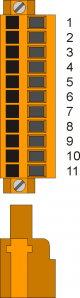
2.3 Digital outputs
2.3.1 8 protected digital outputs
| CN15 | Terminal | Symbol | Description | Address |
|---|---|---|---|---|
| | 1 | V+ | Outputs power in (12-28Vdc) | |
| 2 | O1 | Digital output 1 | 3.OUT01 | |
| 3 | O2 | Digital output 2 | 3.OUT02 | |
| 4 | N.C. | |||
| 5 | O3 | Digital output 3 | 3.OUT03 | |
| 6 | O4 | Digital output 4 | 3.OUT04 | |
| 7 | V- | Outputs power in (12-28Vdc) | ||
| 8 | O5 | Digital output 5 | 3.OUT05 | |
| 9 | O6 | Digital output 6 | 3.OUT06 | |
| 10 | O7 | Digital output 7 | 3.OUT07 | |
| 11 | O8 | Digital output 8 | 3.OUT08 |
2.3.2 4 STEP-DIRECTION outputs
| The electrical features are given in paragraph Electrical features. The wiring examples are given in paragraph Connection examples |
|---|
| CN13 | Terminal | Symbol | Description | Address | |
|---|---|---|---|---|---|
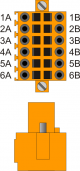 | 1A | VD1 | n.c. | ||
| 2A | DIR1+ | DIRECTION output 1 | Push-Pull Line Driver | 3.PULSE01 | |
| 3A | STEP1+ | STEP output 1 | |||
| 4A | DIR2+ | DIRECTION output 2 | 3.PULSE02 | ||
| 5A | STEP2+ | STEP output 2 | |||
| 6A | 0V | Common for stepper outputs | |||
| 1B | VD1 | n.c. | |||
| 2B | DIR1- | Complementary DIRECTION output 1 | Complementary outputs for use in drives with Line-Driver inputs | ||
| 3B | STEP1- | Complementary output STEP 1 | |||
| 4B | DIR2- | Complementary output DIRECTION 2 | |||
| 5B | STEP2- | Complementary output STEP 2 | |||
| 6B | 0V | Common for stepper outputs | |||
| CN14 | Terminal | Symbol | Description | Address | |
|---|---|---|---|---|---|
| | 1A | VD1 | n.c. | ||
| 2A | DIR1+ | DIRECTION output 3 | Push-Pull Line Driver | 3.PULSE03 | |
| 3A | STEP1+ | STEP output 3 | |||
| 4A | DIR2+ | DIRECTION output 4 | 3.PULSE04 | ||
| 5A | STEP2+ | STEP output 4 | |||
| 6A | 0V | Common for stepper outputs | |||
| 1B | VD1 | n.c. | |||
| 2B | DIR1- | Complementary output DIRECTION 3 | Complementary outputs for use in drives with Line-Driver inputs | ||
| 3B | STEP1- | Uscita complementare STEP 3 | |||
| 4B | DIR2- | Complementary output DIRECTION 4 | |||
| 5B | STEP2- | Complementary output STEP 4 | |||
| 6B | 0V | Common for stepper outputs | |||
2.4 Analog outputs
2.4.1 4 analog outputs +/-10V, 16bit
| The electrical features are given in paragraph Electrical features. The wiring examples are given in paragraph Connection examples |
|---|
| CN16 | Terminal | Symbol | Description | Address |
|---|---|---|---|---|
 | 1 | GAO | Common for analog outputs | |
| 2 | AO1 | Analog output 1 | 3.AN01 | |
| 3 | AO2 | Analog output 2 | 3.AN02 | |
| 4 | GAO | Common for analog outputs | ||
| 5 | AO3 | Analog output 3 | 3.AN03 | |
| 6 | AO4 | Analog output 4 | 3.AN04 |
3. Connection examples
3.1 Digital inputs

3.2 Line Driver counter inputs

3.3 PNP / Push Pull counter inputs

3.4 Voltmetric and amperometric analog inputs

3.5 Voltmetric and potentiometric analog inputs

3.6 Protected digital outputs

3.7 Uscite STEP - DIRECTION

3.8 Analog outputs

4. Electrical features
The following are the electrical hardware.
The maximum and minimum frequency values and actual acquisition times, can still depend on any additional software filters, see the system variable “QMOVE:sys004”.
4.0.1 Ingressi digitali standard
| Tipo | Sinking (PNP) |
| Tempo min. di acquisizione (hardware) | 3ms |
| Tensione di funzionamento nominale | 12÷24Vdc |
| Tensione stato logico 0 | 0÷2 V |
| Tensione stato logico 1 | 10,5 ÷ 26,5 V |
| Corrente assorbita | 2mA@10.5V / 8mA@26.5V |

4.0.2 Ingressi digitali veloci
| Tipo di polarizzazione | NPN / PNP |
| Frequenza massima | 200KHz |
| Tempo min. di acquisizione (hardware) | 5µs |
| Isolamento | 1000Vrms |
| Tensione di funzionamento nominale | 24Vdc |
| Tensione stato logico 0 | 0÷2 V |
| Tensione stato logico 1 | 10,5 ÷ 26,5 V |
| Caduta di tensione interna | 1,2 V |
| Resistenza di ingresso | 2700Ω |

4.0.3 Ingressi di conteggio bidirezionale a 200KHz
I valori riportati in tabella si riferiscono ai segnali d'ingresso A, B e Z.
Il valore di frequenza massima, riportato in tabella si riferisce a dei segnali delle fasi A e B con un DutyCycle = 50%
Con frequenze di conteggio superiori ai 50KHz è preferibile l'uso di encoder di tipo Line-Driver.
| Tipo di polarizzazione | PNP/PP |
| Frequenza massima | 200KHz |
| Tempo min. di acquisizione | 5µs |
| Isolamento | 1000Vrms |
| Tensione di funzionamento nominale | 24Vdc |
| Tensione stato logico 0 | 0 ÷ 2 V |
| Tensione stato logico 1 | 10,5 ÷ 26,5 V |
| Caduta di tensione interna | 1,2V |
| Resistenza di ingresso | 3000Ω |
Line-Driver
| Tipo di polarizzazione | Line-Driver |
| Frequenza massima | 200KHz |
| Tempo min. di acquisizione | 5µs |
| Isolamento | 1000Vrms |
| Tensione di funzionamento nominale (PHx+ ⇔ PHx-) | 5Vdc |
| Tensione stato logico 0 (PHx+ ⇔ PHx-) | 0÷1,5 V |
| Tensione stato logico 1 (PHx+ ⇔ PHx-) | 2÷5 V |
| Caduta di tensione interna | 1,2V |
| Resistenza di ingresso | 150Ω |

4.0.4 Ingressi analogici potenziometrici
| Tipo di collegamento | Potenziometrico 1KΩ÷20KΩ |
| Risoluzione | 12bit/16bit |
| Tensione di riferimento erogata | 2,5Vdc |
| Corrente massima erogata dal riferimento | 10mA |
| Resistenza d'ingresso | 10MΩ |
| Max. errore di linearità | + 0,1% Vfs |
| Max. errore di offset | + 0,1% Vfs |
| S.n. | 71 dB |
| Velocità di aggiornamento | 1ms |
| Isolamento | 1000 Vrms |

4.0.5 Ingressi analogici voltmetrici
| Tipo di collegamento | Voltmetrico 0÷10V |
| Risoluzione | 12bit/16bit |
| Resistenza d'ingresso (Rin) | 20KΩ |
| Valore di danneggiamento | 20V |
| Max. errore di linearità | + 0,1% Vfs |
| Max. errore di offset | + 0,1% Vfs |
| S.n. | 71 dB |
| Velocità di aggiornamento | 1ms |
| Isolamento | 1000 Vrms |

4.0.6 Ingressi analogici amperometrici
| Tipo di collegamento | Amperometrico (0-20 mA) |
| Risoluzione | 12bit/16bit |
| Resistenza d'ingresso | 125Ω |
| Valore di danneggiamento | 25 mA |
| Max. errore di linearità | + 0,1% Vfs |
| Max. errore di offset | + 0,1% Vfs |
| S.n. | 71 dB |
| Velocità di aggiornamento | 1ms |
| Isolamento | 1000 Vrms |

4.0.7 Uscite digitali protette
| Carico commutabile | Dc (PNP) |
| Max. tensione di funzionamento | 28V |
| Isolamento | 1000Vpp |
| Caduta di tensione interna max. | 600mV |
| Resistenza interna massima @ON | 90mΩ |
| Corrente max. di protezione | 12A |
| Corrente max. di funzionamento | 2A |
| Corrente max. @OFF | 5µA |
| Tempo di massimo commutazione da ON a OFF | 270µs |
| Tempo di massimo commutazione da OFF a ON | 250µs |

4.0.8 Uscite per motore stepper
| Tipo di polarizzazione | Push-Pull / Line-Driver |
| Massima frequenza d'uscita | 300KHz |
| Isolamento | 1000Vpp |
| Corrente max. di funzionamento | 20mA |
| Tensione nominale | 12Vdc1) |
1)
Salvo diverse configurazioni

4.0.9 Uscite analogiche
| Tipo di collegamento | In modo comune |
| Isolamento | 1000Vrms |
| Range di tensione (minimo a vuoto) | -9,8V ÷ +9,8V |
| Max. variazione offset in funzione della temperatura | +/- 5mV |
| Risoluzione | 16bit |
| Corrente massima | 1mA |
| Variazione dell'uscita in funzione del carico | 100 µV/mA |
| Resistenza d'uscita | 249Ω |
