
Specialization card 1MS3F rel.01

Informations
| |
||||
| Document: | MIM1MS3F02 | |||
|---|---|---|---|---|
| Description: | Installation and maintenance manual | |||
| Editor: | Riccardo Furlato | |||
| Approver: | Gabriele Bazzi | |||
| Link: | http://www.qem.eu/doku/doku.php/en/strumenti/qmoveplus/mim1MS3F01 | |||
| Language: | English | |||
| Document release | Hardware Release | Description | Note | Date |
| 00 | 01 | New manual | 14/01/2016 | |
1. Description
The 1MS3F is ths card of QCNC1 series.
1.1 Equipment
 | 8 digital inputs 5÷24V |
 | 1 counter input A-B 15KHz |
 | 4 STEP-DIRECTION outputs |
2. Connections
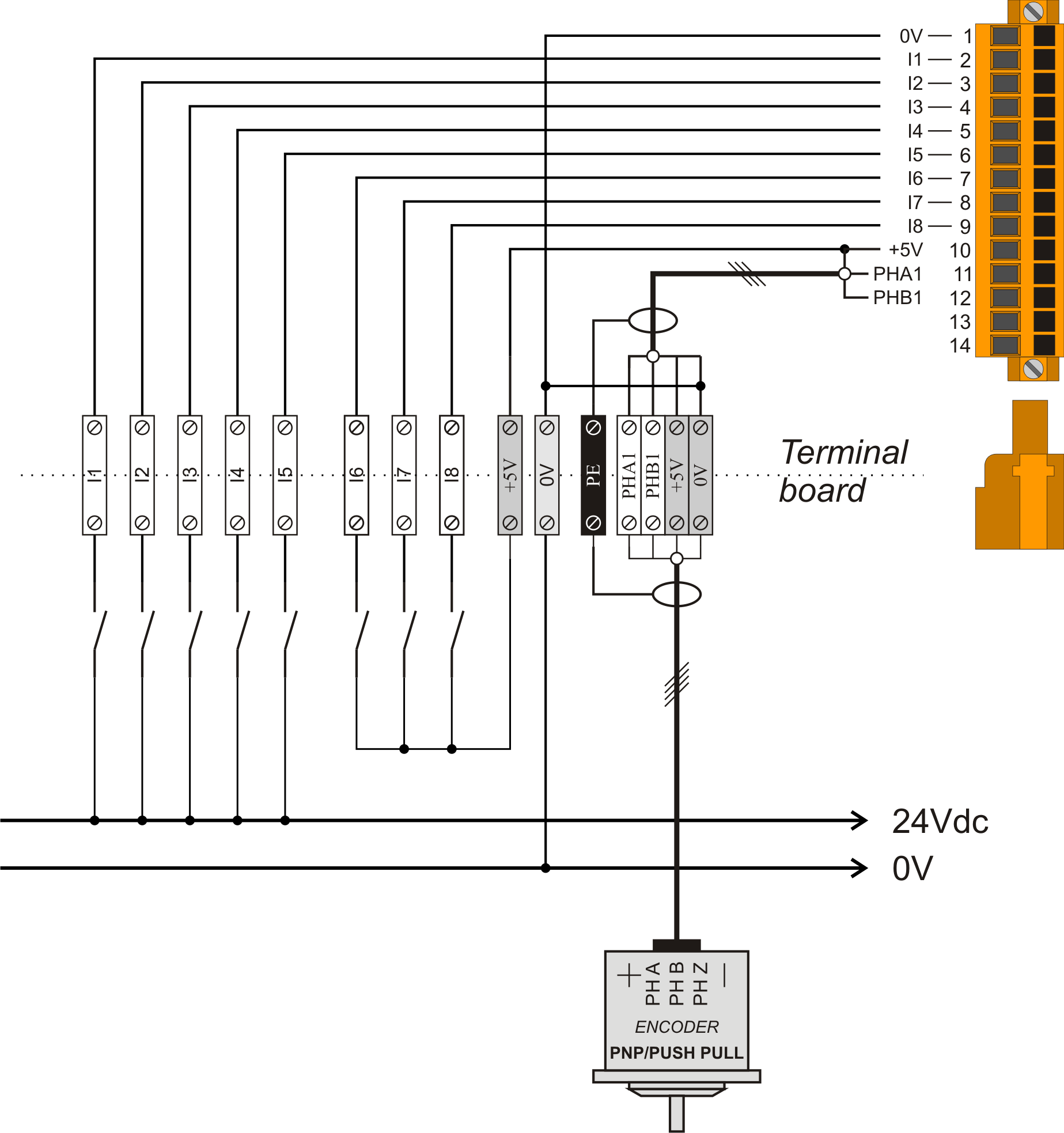
2.1 Digital inputs
2.1.1 8 digital inputs and 1 counter AB
| CN11 | Terminal | Symbol | Description | Address | |
|---|---|---|---|---|---|
 | 1 | 0V | Common of digital inputs | ||
| 2 | I1 | Input 1 | 3.INP01 | ||
| 3 | I2 | Input 2 | 3.INP02 | ||
| 4 | I3 | Input 3 | 3.INP03 | ||
| 5 | I4 | Input 4 | 3.INP04 | ||
| 6 | I5 | Input 5 | 3.INP05 | ||
| 7 | I6 | Input 6 | 3.INP06 | ||
| 8 | I7 | Input 7 | 3.INP07 | ||
| 9 | I8 | Input 8 | 3.INP08 | ||
| 10 | +5V | 5 Volts DC output 1) | |||
| 11 | PHA1 | A phase encoder | 3.CNT05 | 3.INP09 | |
| 12 | PHB1 | B phase encoder | 3.INP10 | ||
| 13 | Internal bridge 13 -14 | ||||
| 14 | |||||
1)
Maximum current 50mA
2.2 Digital outputs
2.2.1 4 STEP-DIRECTION outputs
 | The electrical features are given in sectionElectrical features. The example of the connection are given in section Connection examples |
|---|
.
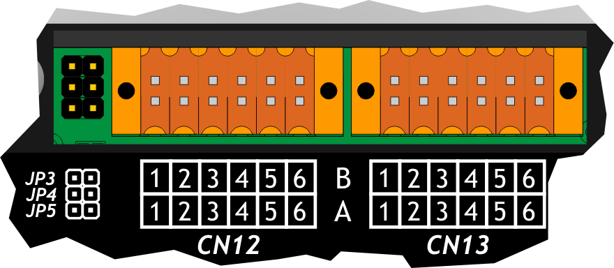
| CN12 | Terminal | Symbol | Description | Address | |
|---|---|---|---|---|---|
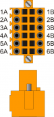 | 1A | VD1 | Internal bridge 1A -1B | ||
| 2A | DIR1+ | DIRECTION 1 output | Push-Pull Line Driver | 3.PULSE01 | |
| 3A | STEP1+ | STEP 1 output | |||
| 4A | DIR2+ | DIRECTION 2 output | 3.PULSE02 | ||
| 5A | STEP2+ | STEP 2 output | |||
| 6A | 0V | Commnon stepper outputs | |||
| 1B | VD1 | Internal bridge 1A -1B | |||
| 2B | DIR1- | DIRECTION 1 complementary output | Complementary outputs for use on driver with Line-Driver inputs | ||
| 3B | STEP1- | STEP 1 complementary output | |||
| 4B | DIR2- | DIRECTION 2 complementary output | |||
| 5B | STEP2- | STEP 2 complementary output | |||
| 6B | 0V | Commnon stepper outputs | |||
.
| CN13 | Terminal | Siymbol | Description | Address | |
|---|---|---|---|---|---|
| | 1A | VD1 | Internal bridge 1A -1B | ||
| 2A | DIR3+ | DIRECTION 3 output | Push-Pull Line Driver | 3.PULSE03 | |
| 3A | STEP3+ | STEP 3 output | |||
| 4A | DIR4+ | DIRECTION 4 output | 3.PULSE04 | ||
| 5A | STEP4+ | STEP 4 output | |||
| 6A | 0V | Commnon stepper outputs | |||
| 1B | VD1 | n.c. | |||
| 2B | DIR3- | DIRECTION 3 complementary output | Complementary outputs for use on driver with Line-Driver inputs | ||
| 3B | STEP3- | STEP 3 complementary output | |||
| 4B | DIR4- | DIRECTION 4 complementary output | |||
| 5B | STEP4- | STEP 4 complementary output | |||
| 6B | 0V | Commnon stepper outputs | |||
STEP-DIRECTION voltage settings
Set JP3, JP4 or JP5 jumper for choose the STEP DIRECTION voltage outputs.
 | Must be inserted only one bridge at a time If you set the 5V(JP5) or 12V(JP3) voltage, the terminal 1A and 1B must be disconnected |
|---|
.
| Nome jumper | Impostazione | Tensione nominale | |
|---|---|---|---|
 | JP3 | INSERTED | 12V (Voltage supplied by the device) |
| JP4 | INSERTED | VD1 (Voltage to be supplied to terminals 1A or 1B) | |
| JP5 | INSERTED | 5V (Voltage supplied by the device) |
.
 | JP3 |
| JP4 | |
| JP5 |
3. Connection examples
3.1 Digital inputs
Example with 5 inputs 24Vdc, 3 inputs 5Vdc and 1 Push-pull encoder 5Vdc
3.2 STEP - DIRECTION outputs

 | JP3 |
| JP4 | |
| JP5 |
4. Electrical features
The following are the electrical hardware features.
The maximum and minimum frequency values and actual acquisition times, can still depend on any additional software filters, see the system variable “QMOVE:sys004”.
4.1 Ingressi
4.1.1 Digital inputs
| Polarization type | PNP |
| Minimum time of acquisition (hardware) | 1ms |
| Insulation | 1000Vrms |
| Nominal working voltage | 5÷24Vdc |
| Maximum applicable voltage | 26Vdc |
| Logical state voltage 0 | < 1.8V |
| Logical state voltage 1 | > 4.5V |
| Internal voltage drop | 5V |
| Input resistance (Ri) | 11200O |
| Maximum absorbed current | 17mA @ 24V |
| Maximum supply current da +5V | 50mA |
4.1.2 Counter input
| The values given in the table refer to A, B e Z input signals. The maximum frequency value, given on the table refer to A e B phase input signal with DutyCycle = 50% With counter frequencies more than 50KHz is preferable to the use of Line-Driver encoders . |
|---|
.
| Polarization type | PNP/PP |
| Maximum frequency | 15KHz |
| Minimum time of acquisition |  |
| Insulation | 1000Vrms |
| Nominal working voltage | 5Vdc |
| Logical state voltage 0 | |
| Logical state voltage 1 | |
| Internal voltage drop | 1.2V |
| Input resistance | 1200O |
4.2 STEP-DIRECTION outputs
| Polarization type | Push-Pull / Line-Driver |
| Maximum output frequency | 300KHz |
| Insulation | 1000Vpp |
| Max working current | 20mA |
| Rated voltage | Selectable with JP3-JP4-JP5 |
