This is an old revision of the document!

Specialization card 1MS3F rel.01

Informations
| |
||||
| Document: | MIM1MS3F02 | |||
|---|---|---|---|---|
| Description: | Installation and maintenance manual | |||
| Editor: | Riccardo Furlato | |||
| Approver: | Gabriele Bazzi | |||
| Link: | http://www.qem.eu/doku/doku.php/strumenti/qmoveplus/mim1MS3F01 | |||
| Language: | English | |||
| Document release | Hardware Release | Description | Note | Date |
| 00 | 01 | New manual | 14/01/2016 | |
1. Description
The 1MS3F is ths card of QCNC1 series.
1.1 Equipment
 | 8 digital inputs 5÷24V |
 | 1 counter input A-B 15KHz |
 | 4 STEP-DIRECTION outputs |
2. Connections
2.1 Digital inputs
2.1.1 8 digital inputs and 1 counter AB
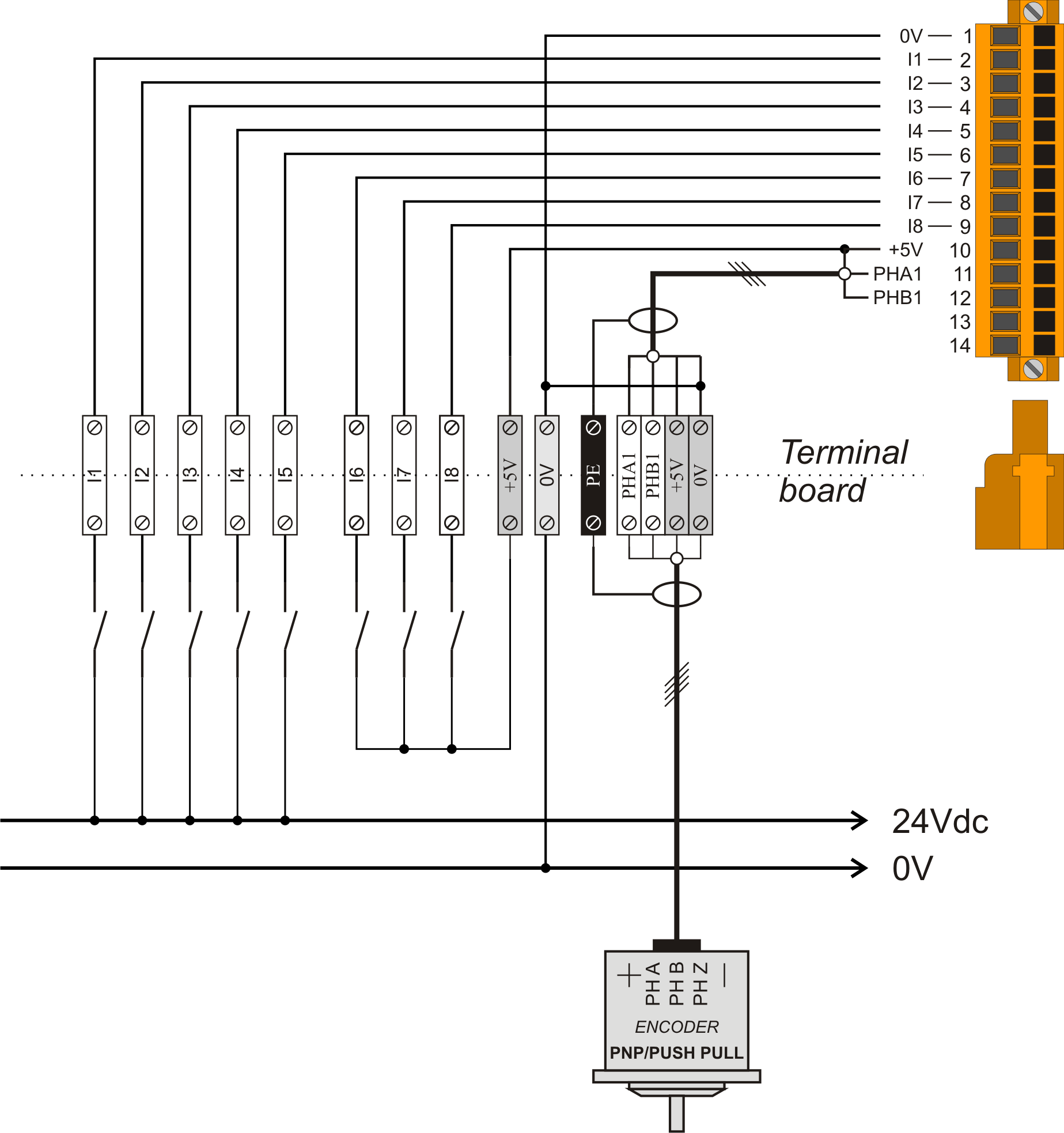
| CN11 | Terminal | Symbol | Description | Address | |
|---|---|---|---|---|---|
 | 1 | 0V | Common of digital inputs | ||
| 2 | I1 | Input 1 | 3.INP01 | ||
| 3 | I2 | Input 2 | 3.INP02 | ||
| 4 | I3 | Input 3 | 3.INP03 | ||
| 5 | I4 | Input 4 | 3.INP04 | ||
| 6 | I5 | Input 5 | 3.INP05 | ||
| 7 | I6 | Input 6 | 3.INP06 | ||
| 8 | I7 | Input 7 | 3.INP07 | ||
| 9 | I8 | Input 8 | 3.INP08 | ||
| 10 | +5V | 5 Volts DC output 1) | |||
| 11 | PHA1 | A phase encoder | 3.CNT05 | 3.INP09 | |
| 12 | PHB1 | B phase encoder | 3.INP10 | ||
| 13 | Internal bridge 13 -14 | ||||
| 14 | |||||
1)
Maximum current 50mA
2.2 Digital outputs
2.2.1 4 STEP-DIRECTION outputs
 | The electrical features are given in sectionElectrical features. The example of the connection are given in section Connection examples |
|---|
.
| CN12 | Terminal | Symbol | Description | Address | |
|---|---|---|---|---|---|
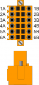 | 1A | VD1 | Internal bridge 1A -1B | ||
| 2A | DIR1+ | DIRECTION 1 output | Push-Pull Line Driver | 3.PULSE01 | |
| 3A | STEP1+ | STEP 1 output | |||
| 4A | DIR2+ | DIRECTION 2 output | 3.PULSE02 | ||
| 5A | STEP2+ | STEP 2 output | |||
| 6A | 0V | Commnon stepper outputs | |||
| 1B | VD1 | Internal bridge 1A -1B | |||
| 2B | DIR1- | DIRECTION 1 complementary output | Complementary outputs for use on driver with Line-Driver inputs | ||
| 3B | STEP1- | STEP 1 complementary output | |||
| 4B | DIR2- | DIRECTION 2 complementary output | |||
| 5B | STEP2- | STEP 2 complementary output | |||
| 6B | 0V | Commnon stepper outputs | |||
.
| CN13 | Terminal | Siymbol | Description | Address | |
|---|---|---|---|---|---|
| | 1A | VD1 | Internal bridge 1A -1B | ||
| 2A | DIR3+ | DIRECTION 3 output | Push-Pull Line Driver | 3.PULSE03 | |
| 3A | STEP3+ | STEP 3 output | |||
| 4A | DIR4+ | DIRECTION 4 output | 3.PULSE04 | ||
| 5A | STEP4+ | STEP 4 output | |||
| 6A | 0V | Commnon stepper outputs | |||
| 1B | VD1 | n.c. | |||
| 2B | DIR3- | DIRECTION 3 complementary output | Complementary outputs for use on driver with Line-Driver inputs | ||
| 3B | STEP3- | STEP 3 complementary output | |||
| 4B | DIR4- | DIRECTION 4 complementary output | |||
| 5B | STEP4- | STEP 4 complementary output | |||
| 6B | 0V | Commnon stepper outputs | |||
STEP-DIRECTION voltage settings
Set JP3, JP4 or JP5 jumper for choose the STEP DIRECTION voltage outputs.
 | Must be inserted only one bridge at a time If you set the 5V(JP5) or 12V(JP3) voltage, the terminal 1A and 1B must be disconnected |
|---|
.
| Nome jumper | Impostazione | Tensione nominale | |
|---|---|---|---|
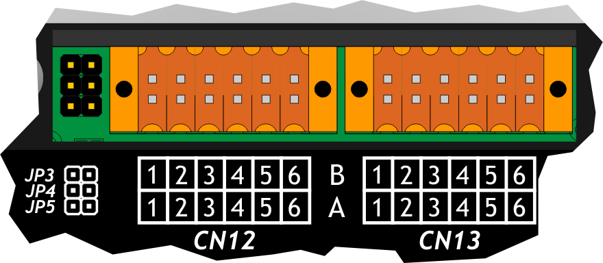 | JP3 | INSERTED | 12V (Voltage supplied by the device) |
| JP4 | INSERTED | VD1 (Voltage to be supplied to terminals 1A or 1B) | |
| JP5 | INSERTED | 5V (Voltage supplied by the device) |
.
 | JP3 |
| JP4 | |
| JP5 |
3. Esempi di collegamento
3.1 Ingressi digitali
Esempio con 5 ingressi 24Vdc, 3 ingressi 5Vdc e 1 encoder Push-pull 5Vdc
3.2 Uscite STEP - DIREZIONE

 | JP3 |
| JP4 | |
| JP5 |
4. Caratteristiche elettriche
Di seguito sono riportate le caratteristiche elettriche hardware.
I valori di frequenze massime e minime e tempi di acquisizione effettivi, possono comunque dipendere da eventuali filtri software aggiuntivi, vedere per esempio la variabile di sistema “QMOVE:sys004”.
4.1 Ingressi
4.1.1 Ingressi digitali
| Tipo di polarizzazione | PNP |
| Tempo min. di acquisizione (hardware) | 1ms |
| Isolamento | 1000Vrms |
| Tensione di funzionamento nominale | 5÷24Vdc |
| Tensione massima applicabile | 26Vdc |
| Tensione stato logico 0 | < 1.8V |
| Tensione stato logico 1 | > 4.5V |
| Caduta di tensione interna | 5V |
| Resistenza di ingresso (Ri) | 11200O |
| Corrente massima assorbita | 17mA @ 24V |
| Corrente massima erogabile da +5V | 50mA |
4.1.2 Ingresso di conteggio
| I valori riportati in tabella si riferiscono ai segnali d'ingresso A, B e Z. Il valore di frequenza massima, riportato in tabella si riferisce a dei segnali delle fasi A e B con un DutyCycle = 50% Con frequenze di conteggio superiori ai 50KHz è preferibile l'uso di encoder di tipo Line-Driver. |
|---|
.
| Tipo di polarizzazione | PNP/PP |
| Frequenza massima | 15KHz |
| Tempo min. di acquisizione |  |
| Isolamento | 1000Vrms |
| Tensione di funzionamento nominale | 5Vdc |
| Tensione stato logico 0 | |
| Tensione stato logico 1 | |
| Caduta di tensione interna | 1.2V |
| Resistenza di ingresso | 1200O |
4.2 STEP-DIRECTION outputs
| Tipo di polarizzazione | Push-Pull / Line-Driver |
| Massima frequenza d'uscita | 300KHz |
| Isolamento | 1000Vpp |
| Corrente max. di funzionamento | 20mA |
| Tensione nominale | Selezionabile con JP3-JP4-JP5 |
